
User Manual


Table Of Contents
- WAFER-945GSE2
- 1 Introduction
- 2 Packing List
- 3 Connectors
- 3.1 Peripheral Interface Connectors
- 3.2 Internal Peripheral Connectors
- 3.2.1 ATX Power Connector
- 3.2.2 ATX Power Supply Enable Connector
- 3.2.3 Audio Connector (10-pin)
- 3.2.4 Backlight Inverter Connector
- 3.2.5 Battery Connector
- 3.2.6 CompactFlash® Socket
- 3.2.7 Digital Input/Output (DIO) Connector
- 3.2.8 Fan Connector (+12V, 3-pin)
- 3.2.9 Keyboard/Mouse Connector
- 3.2.10 LED Connector
- 3.2.11 LVDS LCD Connector
- 3.2.12 PC/104 Connector
- 3.2.13 PC/104 Power Input Connector
- 3.2.14 Power Button Connector
- 3.2.15 Reset Button Connector
- 3.2.16 SATA Drive Connectors
- 3.2.17 Serial Port Connector, RS-232/422/485
- 3.2.18 SPI Flash Connector
- 3.2.19 USB Connectors (Internal)
- 3.3 External Peripheral Interface Connector Panel
- 4 Installation
- 5 BIOS
- 6 Software Drivers
- A BIOS Options
- B One Key Recovery
- C Terminology
- D Digital I/O Interface
- E Watchdog Timer
- F Hazardous Materials Disclosure
WAFER-945GSE2 3.5" Motherboard
Page 23
Pin Description Pin Description
16 A4 41 RESET#
17 A3 42 WAIT#
18 A2 43 INPACK#
19 A1 44 REG#
20 A0 45 BVD2
21 D0 46 BVD1
22 D1 47 D8
23 D2 48 D9
24 IOCS16# 49 D10
25 CD2# 50 GND2
Table 3-8: CF Card Socket Pinouts
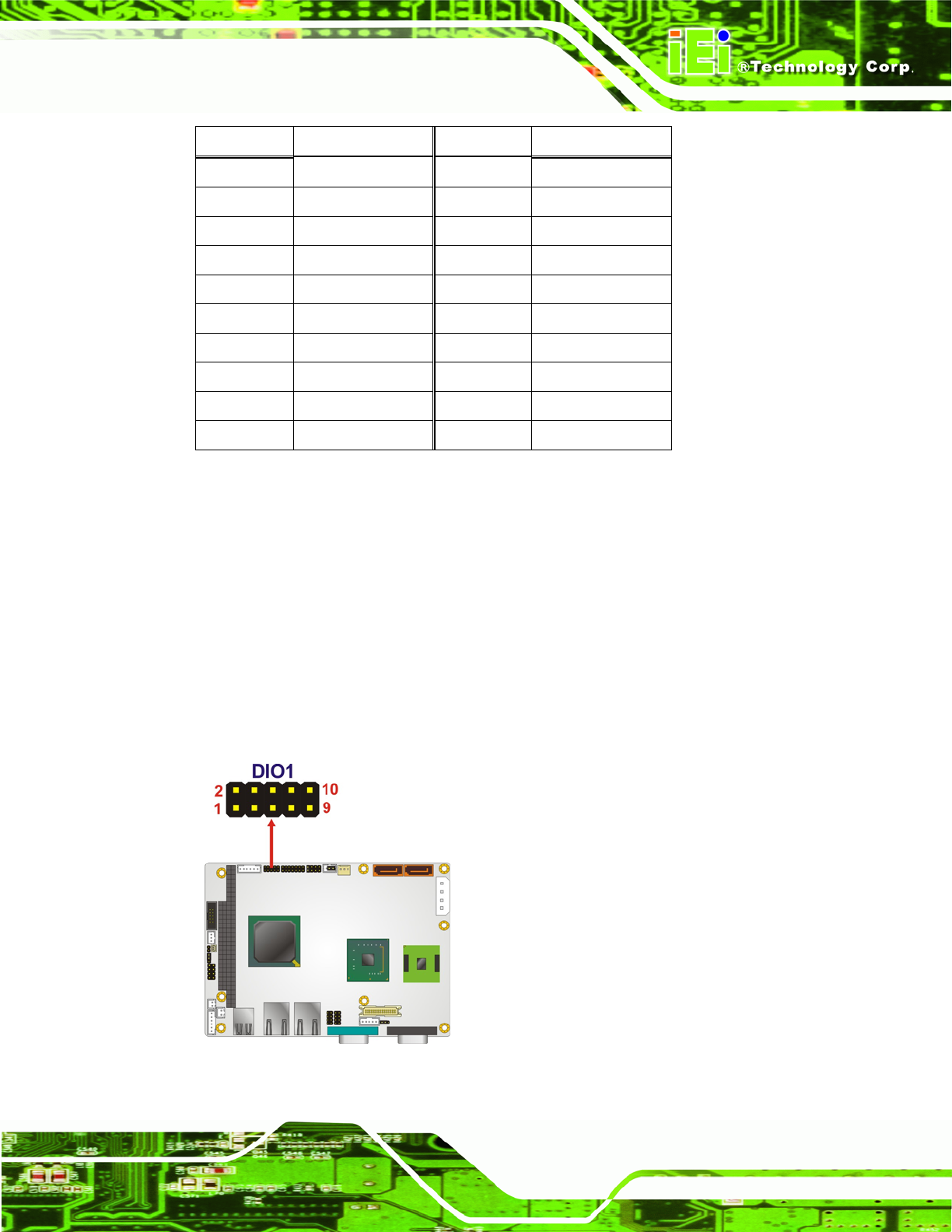
3.2.7 Digital Input/Output (DIO) Connector
CN Label: DIO1
CN Type:
10-pin header
CN Location:
See Figure 3-9
CN Pinouts:
See Table 3-9
The digital input/output connector is managed through a Super I/O chip. The DIO
connector pins are user programmable.
Figure 3-9: Digital I/O Connector Location