
User Manual


Table Of Contents
- WAFER-945GSE2
- 1 Introduction
- 2 Packing List
- 3 Connectors
- 3.1 Peripheral Interface Connectors
- 3.2 Internal Peripheral Connectors
- 3.2.1 ATX Power Connector
- 3.2.2 ATX Power Supply Enable Connector
- 3.2.3 Audio Connector (10-pin)
- 3.2.4 Backlight Inverter Connector
- 3.2.5 Battery Connector
- 3.2.6 CompactFlash® Socket
- 3.2.7 Digital Input/Output (DIO) Connector
- 3.2.8 Fan Connector (+12V, 3-pin)
- 3.2.9 Keyboard/Mouse Connector
- 3.2.10 LED Connector
- 3.2.11 LVDS LCD Connector
- 3.2.12 PC/104 Connector
- 3.2.13 PC/104 Power Input Connector
- 3.2.14 Power Button Connector
- 3.2.15 Reset Button Connector
- 3.2.16 SATA Drive Connectors
- 3.2.17 Serial Port Connector, RS-232/422/485
- 3.2.18 SPI Flash Connector
- 3.2.19 USB Connectors (Internal)
- 3.3 External Peripheral Interface Connector Panel
- 4 Installation
- 5 BIOS
- 6 Software Drivers
- A BIOS Options
- B One Key Recovery
- C Terminology
- D Digital I/O Interface
- E Watchdog Timer
- F Hazardous Materials Disclosure
WAFER-945GSE2 3.5" Motherboard
Page 45
Setting Description
OFF Slave (Default)
Short 1-2 Master
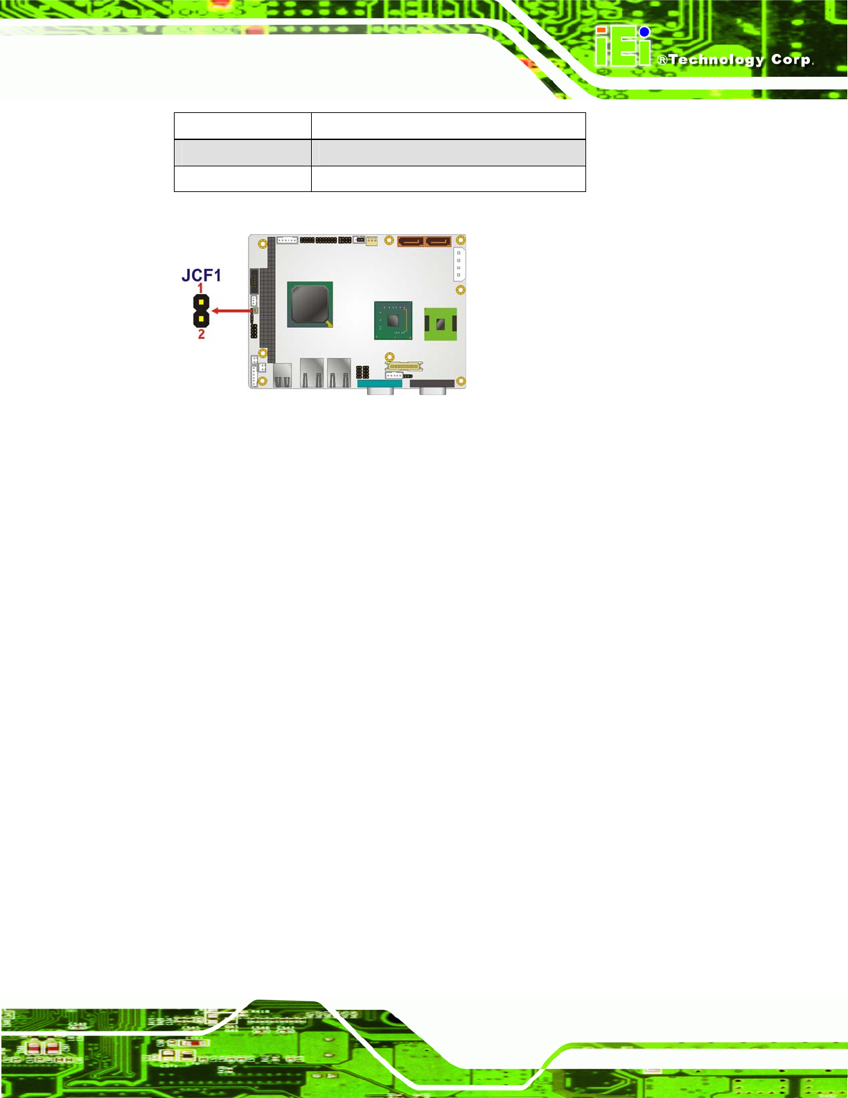
Table 4-3: CF Card Setup Jumper Settings
Figure 4-3: CF Card Setup Jumper Location
4.4.3 Clear CMOS Jumper
Jumper Label: J_CMOS1
Jumper Type:
3-pin header
Jumper Settings:
See Table 4-4
Jumper Location:
See Figure 4-4
If the WAFER-945GSE2 fails to boot due to improper BIOS settings, the clear CMOS
jumper clears the CMOS data and resets the system BIOS information. To do this, use the
jumper cap to close pins 2 and 3 for a few seconds then reinstall the jumper clip back to
pins 1 and 2.
If the “CMOS Settings Wrong” message is displayed during the boot up process, the fault
may be corrected by pressing the F1 to enter the CMOS Setup menu. Do one of the
following:
Enter the correct CMOS setting
Load Optimal Defaults
Load Failsafe Defaults.
After having done one of the above, save the changes and exit the CMOS Setup menu.