
User Manual


Table Of Contents
- WAFER-945GSE2
- 1 Introduction
- 2 Packing List
- 3 Connectors
- 3.1 Peripheral Interface Connectors
- 3.2 Internal Peripheral Connectors
- 3.2.1 ATX Power Connector
- 3.2.2 ATX Power Supply Enable Connector
- 3.2.3 Audio Connector (10-pin)
- 3.2.4 Backlight Inverter Connector
- 3.2.5 Battery Connector
- 3.2.6 CompactFlash® Socket
- 3.2.7 Digital Input/Output (DIO) Connector
- 3.2.8 Fan Connector (+12V, 3-pin)
- 3.2.9 Keyboard/Mouse Connector
- 3.2.10 LED Connector
- 3.2.11 LVDS LCD Connector
- 3.2.12 PC/104 Connector
- 3.2.13 PC/104 Power Input Connector
- 3.2.14 Power Button Connector
- 3.2.15 Reset Button Connector
- 3.2.16 SATA Drive Connectors
- 3.2.17 Serial Port Connector, RS-232/422/485
- 3.2.18 SPI Flash Connector
- 3.2.19 USB Connectors (Internal)
- 3.3 External Peripheral Interface Connector Panel
- 4 Installation
- 5 BIOS
- 6 Software Drivers
- A BIOS Options
- B One Key Recovery
- C Terminology
- D Digital I/O Interface
- E Watchdog Timer
- F Hazardous Materials Disclosure
WAFER-945GSE2 3.5" Motherboard
Page 46
Setting Description
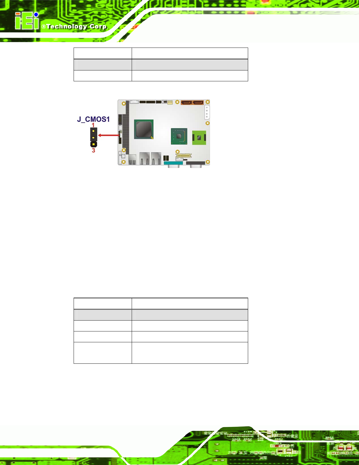
Short 1-2 Keep CMOS Setup (Default)
Short 2-3 Clear CMOS Setup
Table 4-4: Clear BIOS Jumper Settings
Figure 4-4: Clear BIOS Jumper Location
4.4.4 COM 2 Function Select Jumper
Jumper Label: JP1
Jumper Type:
8-pin header
Jumper Settings:
See
Table 4-5
Jumper Location:
See
Figure 4-5
The COM 2 Function Select jumper sets the communication protocol used by the second
serial communications port (COM 2) as RS-232, RS-422 or RS-485.
Setting Description
Short 1-2 RS-232 (Default)
Short 3-4 RS-422
Short 5-6 RS-485
Short 5-6
Short 7-8
RS-485 with RTS control
Table 4-5: COM 2 Function Select Jumper Settings