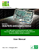
WAFER-945GSELVDS2 IEI Technology Corp. MODEL: WAFER-945GSELVDS2 3.5" SBC with 1.6 GHz Intel® ATOM™ N270 VGA, Dual LVDS, Gigabit Ethernet, CompactFlash® Audio and SATA, RoHS Compliant User Manual Page i Rev. 1.
WAFER-945GSELVDS2 Revision Date Version Changes 12 August, 2011 1.01 Modified SATA connector description 24 September, 2009 1.
WAFER-945GSELVDS2 Copyright COPYRIGHT NOTICE The information in this document is subject to change without prior notice in order to improve reliability, design and function and does not represent a commitment on the part of the manufacturer. In no event will the manufacturer be liable for direct, indirect, special, incidental, or consequential damages arising out of the use or inability to use the product or documentation, even if advised of the possibility of such damages.
WAFER-945GSELVDS2 Table of Contents 1 INTRODUCTION.......................................................................................................... 1 1.1 INTRODUCTION........................................................................................................... 2 1.2 OVERVIEW PHOTO ...................................................................................................... 2 1.3 TECHNICAL SPECIFICATIONS .........................................................................
WAFER-945GSELVDS2 3.3.11 LVDS1 Inverter Connector............................................................................. 26 3.3.12 LVDS2 LCD Connector ................................................................................. 26 3.3.13 LVDS2 Inverter Connector ............................................................................ 28 3.3.14 PCIe Mini Card Slot ...................................................................................... 29 3.3.15 Power Button Connector............
WAFER-945GSELVDS2 4.7.2 Motherboard Installation................................................................................. 56 4.8 INTERNAL PERIPHERAL DEVICE CONNECTIONS ........................................................ 56 4.8.1 Audio Kit Installation....................................................................................... 56 4.8.2 SATA Drive Connection ................................................................................... 57 4.8.3 RS-232 Cable Connection.............
WAFER-945GSELVDS2 5.4 PCI/PNP................................................................................................................... 97 5.5 BOOT........................................................................................................................ 98 5.5.1 Boot Settings Configuration............................................................................. 99 5.5.2 Boot Device Priority ......................................................................................
WAFER-945GSELVDS2 List of Figures Figure 1-1: WAFER-945GSELVDS2...............................................................................................2 Figure 1-2: WAFER-945GSELVDS2 Overview [Front View] .......................................................3 Figure 1-3: Main Dimensions (mm)...............................................................................................5 Figure 1-4: Bottom Dimensions (mm) ..............................................................................
WAFER-945GSELVDS2 Figure 3-25: VGA Connector .......................................................................................................39 Figure 4-1: SO-DIMM Installation ................................................................................................44 Figure 4-2: CF Card Installation ..................................................................................................46 Figure 4-3: AT Power Select Jumper Location....................................................
WAFER-945GSELVDS2 List of Tables Table 1-1: Technical Specifications..............................................................................................4 Table 2-1: Packing List.................................................................................................................11 Table 2-2: Optional Items.............................................................................................................11 Table 3-1: Peripheral Interface Connectors ............................
WAFER-945GSELVDS2 Table 4-1: Jumpers .......................................................................................................................47 Table 4-2: AT Power Select Jumper Settings ............................................................................48 Table 4-3: Audio Power Source...................................................................................................48 Table 4-4: CF Card Setup Jumper Settings ...........................................................
WAFER-945GSELVDS2 BIOS Menus BIOS Menu 1: Main .......................................................................................................................73 BIOS Menu 2: Advanced ..............................................................................................................74 BIOS Menu 3: CPU Configuration ...............................................................................................75 BIOS Menu 4: IDE Configuration................................................
WAFER-945GSELVDS2 Chapter 1 1 Introduction Page 1
WAFER-945GSELVDS2 1.1 Introduction Figure 1-1: WAFER-945GSELVDS2 The WAFER-945GSELVDS2 is a 3.5" motherboard with a 1.6 GHz Intel® ATOM™ N270 processor with 512 KB L2 cache. Also supports one supports one 400 MHz or 533 MHz DDR2 SO-DIMM up to 2.0 GB. The WAFER-945GSELVDS2 has 18-bit and 24-bit dual-channel LVDS connectors, and a single VGA video output. External connectors include USB and Gigabit Ethernet connectors.
WAFER-945GSELVDS2 Figure 1-2: WAFER-945GSELVDS2 Overview [Front View] 1.3 Technical Specifications WAFER-945GSELVDS2 technical specifications are listed in Table 1-1. See Chapter 2 for details. Specification WAFER-945GSELVDS2 Form Factor 3.5" System CPU 1.
WAFER-945GSELVDS2 Specification WAFER-945GSELVDS2 Memory One 200-pin SO-DIMM socket supports one 400 MHz or 533 MHz 2.0 GB (max.) DDR2 SDRAM SO-DIMM CompactFlash® One CompactFlash® Type II socket Super I/O ITE IT8718 Display 18-bit dual-channel LVDS 24-bit dual-channel LVDS VGA BIOS AMI Audio Realtek ALC655 AC'97 audio chip LAN 1 x Realtek 8111CP PCIe GbE chips COM 3 x RS-232 serial ports (one external, two internal) 1 x RS-232/422/485 serial port (internal) USB2.
WAFER-945GSELVDS2 1.
WAFER-945GSELVDS2 Figure 1-4: Bottom Dimensions (mm) Figure 1-5: External Interface Panel Dimensions (mm) Page 6
WAFER-945GSELVDS2 1.5 Data Flow Figure 1-6 shows the data flow between the two on-board chipsets and other components installed on the motherboard and described in the following sections of this chapter.
WAFER-945GSELVDS2 Chapter 2 2 Unpacking Page 8
WAFER-945GSELVDS2 2.1 Anti-static Precautions WARNING! Failure to take ESD precautions during the installation of the WAFER-945GSELVDS2 may result in permanent damage to the WAFER-945GSELVDS2 and severe injury to the user. Electrostatic discharge (ESD) can cause serious damage to electronic components, including the WAFER-945GSELVDS2. Dry climates are especially susceptible to ESD.
WAFER-945GSELVDS2 2.3 Unpacking Checklist NOTE: If any of the components listed in the checklist below are missing, do not proceed with the installation. Contact the IEI reseller or vendor the WAFER-945GSELVDS2 was purchased from or contact an IEI sales representative directly by sending an email to sales@iei.com.tw. 2.3.
WAFER-945GSELVDS2 Quantity Item and Part Number 1 Utility CD 1 Quick Installation Guide Image Table 2-1: Packing List 2.3.
WAFER-945GSELVDS2 Chapter 3 3 Connectors Page 12
WAFER-945GSELVDS2 3.1 Peripheral Interface Connectors The connectors on the WAFER-945GSELVDS2 are shown in the diagram below. Figure 3-1: Connector and Jumper Locations [Front Side] 3.2 Peripheral Interface Connectors Table 3-1 shows a list of the peripheral interface connectors on the WAFER-945GSELVDS2. Detailed descriptions of these connectors can be found below. 3.2.
WAFER-945GSELVDS2 Connector Type Label Digital I/O connector 10-pin header DIO1 Fan connector 3-pin wafer CPU_FAN1 Keyboard and mouse connector 6-pin wafer KB_MS1 LED connector 6-pin header LED_C1 LVDS1 connector 30-pin crimp LVDS1 LVDS1 inverter connector 5-pin wafer INVERTER1 LVDS2 connector 30-pin crimp LVDS2 LVDS2 inverter connector 5-pin wafer INVERTER2 PCIe Mini Card slot PCIe Mini Slot CN4 Power Button 2-pin wafer PWRBTN1 Reset button connector 2-pin header RESET1
WAFER-945GSELVDS2 3.3 Internal Peripheral Connectors Internal peripheral connectors are found on the motherboard and are only accessible when the motherboard is outside of the chassis. This section has complete descriptions of all the internal, peripheral connectors on the WAFER-945GSELVDS2. 3.3.1 ATX Power Connector CN Label: ATXPWR1 CN Type: 4-pin AT power connector (1x4) CN Location: See Figure 3-2 CN Pinouts: See Table 3-3 The 4-pin ATX power connector is connected to an ATX power supply.
WAFER-945GSELVDS2 CN Type: 3-pin wafer (1x3) CN Location: See Figure 3-3 CN Pinouts: See Table 3-4 Short pins 2-3 for AT power use, or connect to power control cable for ATX power control use. Figure 3-3: ATX Power Control Connector Location Pin Description 1 +5V Standby 2 GND 3 PS_ON# Table 3-4: ATX Power Supply Enable Connector Pinouts 3.3.
WAFER-945GSELVDS2 See Table 3-5 CN Pinouts: The 10-pin audio connector is connected to external audio devices including speakers and microphones for the input and output of audio signals to and from the system. Figure 3-4: Audio Connector Pinouts Pin Description Pin Description 1 Line out R 2 Line in R 3 GND 4 GND 5 Line out L 6 Line in L 7 GND 8 GND 9 MIC in 10 Mic in Table 3-5: Audio Connector Pinouts 3.3.
WAFER-945GSELVDS2 CN Label: BAT1 CN Type: 2-pin wafer (1x2) CN Location: See Figure 3-5 CN Pinouts: See Table 3-6 This is connected to the system battery. The battery provides power to the system clock to retain the time when power is turned off. Figure 3-5: Battery Connector Location Pin Description 1 Battery+ 2 Ground Table 3-6: Battery Connector Pinouts 3.3.
WAFER-945GSELVDS2 Figure 3-6: CF Card Slot Location Pin Description Pin Description 1 GND 26 CD1# 2 D3 27 D11 3 D4 28 D12 4 D5 29 D13 5 D6 30 D14 6 D7 31 D15 7 CE# 32 CE2# 8 A10 33 VS1# 9 OE# 34 IOR# 10 A9 35 IOW# 11 A8 36 WE# 12 A7 37 IRQ 13 VCC 38 VCC 14 A6 39 CSEL# 15 A5 40 VS2# Page 19
WAFER-945GSELVDS2 Pin Description Pin Description 16 A4 41 RESET# 17 A3 42 WAIT# 18 A2 43 INPACK# 19 A1 44 REG# 20 A0 45 BVD2 21 D0 46 BVD1 22 D1 47 D8 23 D2 48 D9 24 IOCS16# 49 D10 25 CD2# 50 GND2 Table 3-7: CF Card Slot Pinouts 3.3.6 Digital I/O Connector CN Label: DIO1 CN Type: 10-pin header (2x5) CN Location: See Figure 3-7 CN Pinouts: See Table 3-8 The digital input/output connector is managed through a Super I/O chip.
WAFER-945GSELVDS2 Figure 3-7: Digital I/O Connector Location Pin Description Pin Description 1 GND 2 VCC 3 Output 3 4 Output 2 5 Output 1 6 Output 0 7 Input 3 8 Input 2 9 Input 1 10 Input 0 Table 3-8: Digital I/O Connector Location 3.3.7 CPU Fan Connector CN Label: CPU_FAN1 CN Type: 3-pin header CN Location: See Figure 3-8 CN Pinouts: See Table 3-9 Connects to a CPU fan.
WAFER-945GSELVDS2 Figure 3-8: CPU Fan Connector Location Pin Description 1 GND 2 +12V 3 Fan Speed Detect Table 3-9: CPU Fan Connector Pinouts 3.3.8 Keyboard/Mouse Connector CN Label: KB_MS1 CN Type: 6-pin header (1x6) CN Location: See Figure 3-9 CN Pinouts: See Table 3-10 The keyboard and mouse connector can be connected to a standard PS/2 cable or PS/2 Y-cable to add keyboard and mouse functionality to the system.
WAFER-945GSELVDS2 Figure 3-9: Keyboard/Mouse Connector Location Pin Description 1 VCC (+5 V) 2 MS DATA 3 MS CLK 4 KB DATA 5 KB CLK 6 GROUND Table 3-10: Keyboard/Mouse Connector Pinouts 3.3.9 LED Connector CN Label: LED_C1 CN Type: 6-pin wafer (1x6) CN Location: See Figure 3-10 CN Pinouts: See Table 3-11 The LED connector connects to an HDD indicator LED and a power LED on the system chassis to inform the user about HDD activity and the power on/off status of the system.
WAFER-945GSELVDS2 Figure 3-10: LED Connector Locations Pin Description 1 +5V 2 GND 3 Power LED+ 4 Power LED- 5 HDD LED+ 6 HDD LED- Table 3-11: LED Connector Pinouts 3.3.10 LVDS1 LCD Connector CN Label: LVDS1 CN Type: 30-pin crimp (2x15) CN Location: See Figure 3-11 CN Pinouts: See Table 3-12 The 18-bit, dual-channel LVDS connector can be attached to any compatible LVDS monitor.
WAFER-945GSELVDS2 Figure 3-11: LVDS1 Location Pin Description Pin Description 1 GND1 2 GND2 3 A_Y0 4 A_Y0# 5 A_Y1 6 A_Y1# 7 A_Y2 8 A_Y2# 9 A_CK 10 A_CK# 11 NC 12 NC 13 GND3 14 GND4 15 B_Y0 16 B_Y0# 17 B_Y1 18 B_Y1# 19 B_Y2 20 B_Y2# 21 B_CK 22 B_CK# 23 NC 24 NC 25 GND5 26 GND6 27 VCC_LCD 28 VCC_LCD 29 VCC_LCD 30 VCC_LCD Table 3-12: LVDS1 Pinouts Page 25
WAFER-945GSELVDS2 3.3.11 LVDS1 Inverter Connector CN Label: INVERTER1 CN Type: 5-pin wafer (1x5) CN Location: See Figure 3-12 CN Pinouts: See Table 3-13 Provides power to an LVDS monitor. Figure 3-12: Backlight Connector Pinout Locations Pin Description 1 LCD Backlight Control 2 GROUND 3 +12V 4 GROUND 5 BACKLIGHT Enable Table 3-13: Backlight Connector Pinouts 3.3.
WAFER-945GSELVDS2 CN Pinouts: See Table 3-14 The 18-bit, dual-channel LVDS connector can be attached to any compatible LVDS monitor.
WAFER-945GSELVDS2 Pin Description Pin Description 29 VCC_LCD 30 VCC_LCD Table 3-14: LVDS2 Pinouts 3.3.13 LVDS2 Inverter Connector CN Label: INVERTER2 CN Type: 5-pin wafer (1x5) CN Location: See Figure 3-12 CN Pinouts: See Table 3-13 Provides power to an LVDS monitor.
WAFER-945GSELVDS2 Pin Description 5 BACKLIGHT Enable Table 3-15: Backlight Connector Pinouts 3.3.14 PCIe Mini Card Slot CN Label: CN4 CN Type: 52-pin Mini PCIe Card Slot CN Location: See Figure 3-15 CN Pinouts: See Table 3-16 The PCIe mini card slot enables a PCIe mini card expansion module to be connected to the board. Cards supported include among others wireless LAN (WLAN) cards.
WAFER-945GSELVDS2 Pin Description Pin Description 7 CLKREQ# 8 N/C 9 GND 10 N/C 11 CLK- 12 N/C 13 CLK+ 14 N/C 15 GND 16 N/C 17 N/C 18 GND 19 N/C 20 VCC3 21 GND 22 PCIRST# 23 PERN2 24 3VDual 25 PERP2 26 GND 27 GND 28 1.5V 29 GND 30 SMBCLK 31 PETN2 32 SMBDATA 33 PETP2 34 GND 35 GND 36 USBD- 37 N/C 38 USBD+ 39 N/C 40 GND 41 N/C 42 N/C 43 N/C 44 RF_LINK# 45 N/C 46 BLUELED# 47 N/C 48 1.
WAFER-945GSELVDS2 Turns the system on and off when the system is set to ATX power mode. Figure 3-16: Power Button Connector Location Pin Description 1 Power Switch 2 GND Table 3-17: Power Button Connector Pinouts 3.3.16 Reset Button Connector CN Label: RESET1 CN Type: 2-pin wafer (1x2) CN Location: See Figure 3-17 CN Pinouts: See Table 3-18 Used to reset the system when set to use ATX power.
WAFER-945GSELVDS2 Figure 3-17: Reset Button Connector Locations Pin Description 1 Reset Switch 2 GND Table 3-18: Reset Button Connector Pinouts 3.3.17 SATA Drive Connectors CN Label: SATA1, SATA2 CN Type: 7-pin SATA drive connectors CN Location: See Figure 3-18 CN Pinouts: See Table 3-19 The SATA drive connectors can be connected to SATA drives and support up to 3.0 Gb/s data transfer rate.
WAFER-945GSELVDS2 Figure 3-18: SATA Drive Connector Locations Pin Description 1 GND 2 TX+ 3 TX- 4 GND 5 RX- 6 RX+ 7 GND Table 3-19: SATA Drive Connector Pinouts 3.3.18 Serial Port Connector CN Label: COM3, COM4 CN Type: 10-pin header CN Location: See Figure 3-19 CN Pinouts: See Table 3-20 Provide an RS-232 communications connection.
WAFER-945GSELVDS2 Figure 3-19: Serial Port Connector Location Pin Description Pin Description 1 DCD# 2 DSR# 3 RXD 4 RTS# 5 TXD 6 CTS# 7 DTR# 8 RI# 9 GND 10 GND Table 3-20: Serial Port Pinouts 3.3.19 Serial Port Connector (RS-232/422/485) CN Label: COM2 CN Type: 14-pin header (2x7) CN Location: See Figure 3-20 CN Pinouts: See Table 3-21 The 14-pin serial port connector connects to the COM2 serial communications channels. COM2 is a multi function channel.
WAFER-945GSELVDS2 Figure 3-20: RS-232/422/485 Serial Port Connector Location Pin Description Pin Description 1 DCD# 2 DSR# 3 RXD 4 RTS# 5 TXD 6 CTS# 7 DTR# 8 RI# 9 GND 10 N/C 11 TXD485+ 12 TXD485- 13 RXD485+ 14 RXD485- Table 3-21: RS-232/RS-485 Serial Port Connector Pinouts 3.3.
WAFER-945GSELVDS2 The 2x4 USB pin connectors each provide connectivity to two USB 1.1 or two USB 2.0 ports. Each USB connector can support two USB devices. Additional external USB ports are found on the rear panel. The USB ports are used for I/O bus expansion. Figure 3-21: USB Connector Pinout Locations Pin Description Pin Description 1 VCC 2 GND 3 DATA- 4 DATA+ 5 DATA+ 6 DATA- 7 GND 8 VCC Table 3-22: USB Port Connector Pinouts 3.
WAFER-945GSELVDS2 3.4.1 LAN Connectors CN Label: LAN1 CN Type: RJ-45 CN Location: See Figure 3-22 CN Pinouts: See Table 3-23 The WAFER-945GSELVDS2 is equipped with two built-in RJ-45 Ethernet controllers. The controllers can connect to the LAN through two RJ-45 LAN connectors. There are two LEDs on the connector indicating the status of LAN.
WAFER-945GSELVDS2 3.4.2 Serial Port Connector CN Label: COM1 CN Type: DB-9 connectors CN Location: See Figure 3-22 CN Pinouts: See Table 3-25 and Figure 3-24 The 9-pin DB-9 serial port connectors are connected to RS-232 serial communications devices. Pin Description Pin Description 1 DCD# 6 DSR# 2 RX 7 RTS# 3 TX 8 CTS# 4 DTR# 9 RI# 5 GND Table 3-25: Serial Port Pinouts Figure 3-24: Serial Port Pin Location 3.4.
WAFER-945GSELVDS2 Pin Description Pin Description 1 VCC (+5V) 5 VCC (+5V) 2 DATA4- 6 DATA5- 3 DATA4+ 7 DATA5+ 4 GND 8 GND Table 3-26: USB Port Pinouts 3.4.4 VGA Connector CN Label: VGA1 CN Type: 15-pin Female CN Location: See Figure 3-22 CN Pinouts: See Figure 3-25 and Table 3-27 The WAFER-945GSELVDS2 has a single 15-pin female connector for connectivity to standard display devices.
WAFER-945GSELVDS2 Chapter 4 4 Installation Page 40
WAFER-945GSELVDS2 4.1 Anti-static Precautions WARNING: Failure to take ESD precautions during the installation of the WAFER-945GSELVDS2 may result in permanent damage to the WAFER-945GSELVDS2 and severe injury to the user. Electrostatic discharge (ESD) can cause serious damage to electronic components, including the WAFER-945GSELVDS2. Dry climates are especially susceptible to ESD.
WAFER-945GSELVDS2 4.2 Installation Considerations NOTE: The following installation notices and installation considerations should be read and understood before the WAFER-945GSELVDS2 is installed. All installation notices pertaining to the installation of the WAFER-945GSELVDS2 should be strictly adhered to. Failing to adhere to these precautions may lead to severe damage of the WAFER-945GSELVDS2 and injury to the person installing the motherboard. 4.2.
WAFER-945GSELVDS2 Turn all power to the WAFER-945GSELVDS2 off: o When working with the WAFER-945GSELVDS2, make sure that it is disconnected from all power supplies and that no electricity is being fed into the system. Before and during the installation of the WAFER-945GSELVDS2 DO NOT: Remove any of the stickers on the PCB board. These stickers are required for warranty validation. Use the product before verifying all the cables and power connectors are properly connected.
WAFER-945GSELVDS2 4.3 Unpacking When the WAFER-945GSELVDS2 is unpacked, please check all the unpacking list items listed in Chapter 3 are indeed present. If any of the unpacking list items are not available please contact the WAFER-945GSELVDS2 vendor reseller/vendor where the WAFER-945GSELVDS2 was purchased or contact an IEI sales representative. 4.4 SO-DIMM Installation WARNING: Using incorrectly specified SO-DIMM may cause permanently damage the WAFER-945GSELVDS2.
WAFER-945GSELVDS2 Step 3: Insert the SO-DIMM. Push the SO-DIMM chip into the socket at an angle. (See Figure 4-1) Step 4: Open the SO-DIMM socket arms. Gently pull the arms of the SO-DIMM socket out and push the rear of the SO-DIMM down. (See Figure 4-1) Step 5: Secure the SO-DIMM. Release the arms on the SO-DIMM socket. They clip into place and secure the SO-DIMM in the socket.Step 0: 4.5 CF Card Installation NOTE: The WAFER-945GSELVDS2 can support both CF Type I cards and CF Type II cards.
WAFER-945GSELVDS2 Figure 4-2: CF Card Installation 4.6 Jumper Settings NOTE: A jumper is a metal bridge used to close an electrical circuit. It consists of two or three metal pins and a small metal clip (often protected by a plastic cover) that slides over the pins to connect them. To CLOSE/SHORT a jumper means connecting the pins of the jumper with the plastic clip and to OPEN a jumper means removing the plastic clip from a jumper.
WAFER-945GSELVDS2 Before the WAFER-945GSELVDS2 is installed in the system, the jumpers must be set in accordance with the desired configuration. The jumpers on the WAFER-945GSELVDS2 are listed in Table 4-1.
WAFER-945GSELVDS2 Pin Description Open Use ATX power Table 4-2: AT Power Select Jumper Settings The location of the AT Power Select jumper is shown in Figure 4-3 below. Figure 4-3: AT Power Select Jumper Location 4.6.2 Audio Power Source Jumper Label: JP2 Jumper Type: 3-pin header Jumper Settings: See Table 4-3 Jumper Location: See Figure 4-4 Sets the power source for the onboard audio.
WAFER-945GSELVDS2 The location of the audio power source selection jumper is shown below. Figure 4-4: Audio Power Source 4.6.3 CF Card Setup Jumper Label: JCF1 Jumper Type: 2-pin header Jumper Settings: See Table 4-4 Jumper Location: See Figure 4-5 The CF Card Setup jumper sets the CF Type I card or CF Type II cards as either the slave device or the master device. CF Card Setup jumper settings are shown in Table 4-4.
WAFER-945GSELVDS2 Figure 4-5: CF Card Setup Jumper Location 4.6.4 Clear CMOS Jumper Jumper Label: J_CMOS1 Jumper Type: 3-pin header Jumper Settings: See Table 4-5 Jumper Location: See Figure 4-6 If the WAFER-945GSELVDS2 fails to boot due to improper BIOS settings, the clear CMOS jumper clears the CMOS data and resets the system BIOS information. To do this, use the jumper cap to close pins 2 and 3 for a few seconds then reinstall the jumper clip back to pins 1 and 2.
WAFER-945GSELVDS2 Pin Description 1-2 Keep CMOS Setup 2-3 Clear CMOS Setup Table 4-5: Clear CMOS Jumper Settings The location of the clear CMOS jumper is shown in Figure 4-6 below. Figure 4-6: Clear CMOS Jumper 4.6.5 COM2 Mode Selection Jumper Label: JP1 Jumper Type: 8-pin header Jumper Settings: See Table 4-6 Jumper Location: See Figure 4-7 The COM 2 Function Select jumper sets the communication protocol used by the second serial communications port (COM 2) as RS-232, RS-422 or RS-485.
WAFER-945GSELVDS2 Figure 4-7: COM 2 Function Select Jumper Location 4.6.6 LVDS1 and LVDS2 Panel Resolution Jumper Jumper Label: J_LCD_TYPE1 Jumper Type: 8-pin header Jumper Settings: See Table 4-7 Jumper Location: See Figure 4-8 Sets the resolution of both LVDS1 and LVDS2 video channels.
WAFER-945GSELVDS2 Figure 4-8:LVDS Panel Resolution Jumper Pinout Locations 4.6.7 LVDS1 Voltage Selection WARNING: Permanent damage to the screen and WAFER-945GSELVDS2 may occur if the wrong voltage is selected with this jumper. Please refer to the user guide that came with the monitor to select the correct voltage. Jumper Label: J_VLVDS1 Jumper Type: 3-pin header Jumper Settings: See Table 4-9 Jumper Location: See Figure 4-9 Sets the voltage provided to the monitor by LVDS1.
WAFER-945GSELVDS2 The LVDS1 Voltage Selection jumper location. is shown in Figure 4-9. Figure 4-9: LVDS1 Voltage Selection Jumper Pinout Locations 4.6.8 LVDS2 Voltage Selection WARNING: Permanent damage to the screen and WAFER-945GSELVDS2 may occur if the wrong voltage is selected with this jumper. Please refer to the user guide that cam with the monitor to select the correct voltage.
WAFER-945GSELVDS2 Figure 4-10: LVDS Voltage Selection Jumper Pinout Locations 4.7 Chassis Installation 4.7.1 Airflow WARNING: Airflow is critical to the cooling of the CPU and other onboard components. The chassis in which the WAFER-945GSELVDS2 must have air vents to allow cool air to move into the system and hot air to move out. The WAFER-945GSELVDS2 must be installed in a chassis with ventilation holes on the sides allowing airflow to travel through the heat sink surface.
WAFER-945GSELVDS2 4.7.2 Motherboard Installation To install the WAFER-945GSELVDS2 motherboard into the chassis please refer to the reference material that came with the chassis. 4.8 Internal Peripheral Device Connections Install the following cables to use the internal devices listed. 4.8.1 Audio Kit Installation The Audio Kit that came with the WAFER-945GSELVDS2 connects to the audio connector on the WAFER-945GSELVDS2. The audio kit consists of three audio jacks. Mic-in connects to a microphone.
WAFER-945GSELVDS2 Figure 4-11: Audio Kit Cable Connection Step 3: Connect the audio devices. Connect speakers to the line-out audio jack. Connect the output of an audio device to the line-in audio jack. Connect a microphone to the mic-in audio jack.Step 0: 4.8.2 SATA Drive Connection The WAFER-945GSELVDS2 is shipped with two SATA drive cables and one SATA drive power cable. To connect the SATA drives to the connectors, please follow the steps below. Step 1: Locate the connectors.
WAFER-945GSELVDS2 Step 2: Insert the cable connector. Press the clip on the connector at the end of the SATA cable and insert the cable connector into the onboard SATA drive connector. See Figure 4-12. Figure 4-12: SATA Drive Cable Connection Step 3: Connect the cable to the SATA disk. Connect the connector on the other end of the cable to the connector at the back of the SATA drive. See Figure 4-13. NOTE: The SATA power cable described below is an optional item and must be pre-ordered.
WAFER-945GSELVDS2 Figure 4-13: SATA Power Drive Connection 4.8.3 RS-232 Cable Connection The dual RS-232 cable consists of two connectors attached to two independent cables. Each cable is then attached to a D-sub 9-pin male connector. To install the dual RS-232 cable, please follow the steps below. Step 1: Locate the connectors. The locations of the RS-232 connectors are shown in Chapter 3. Step 2: Insert the cable connectors. Insert one connector into each serial port box headers. See Figure 5-13.
WAFER-945GSELVDS2 Figure 4-14: Dual RS-232 Cable Installation Step 3: Secure the connectors. Both single RS-232 connectors have two retention screws that must be secured to a chassis or bracket. Step 4: Connect the serial device. Once the single RS-232 connectors are connected to a chassis or bracket, a serial communications device can be connected to the system. Step 0: 4.8.4 Keyboard/Mouse Y-cable Connector The WAFER-945GSELVDS2 is shipped with a keyboard/mouse Y-cable connector.
WAFER-945GSELVDS2 Step 3: Insert the cable connectors. Once the cable connector is properly aligned with the keyboard/mouse connector on the WAFER-945GSELVDS2, connect the cable connector to the on-board connectors. See Figure 4-15. Figure 4-15: Keyboard/mouse Y-cable Connection Step 4: Attach PS/2 connectors to the chassis. The keyboard/mouse Y-cable connector is connected to two PS/2 connectors.
WAFER-945GSELVDS2 4.8.5 USB Cable The WAFER-945GSELVDS2 is shipped with a dual port USB 2.0 cable. To connect the USB cable connector, please follow the steps below. Step 1: Locate the connectors. The locations of the USB connectors are shown in Chapter 3. WARNING: If the USB pins are not properly aligned, the USB device can burn out. Step 2: Align the connectors. The cable has two connectors. Correctly align pin 1on each cable connector with pin 1 on the WAFER-945GSELVDS2 USB connector.
WAFER-945GSELVDS2 4.9 External Peripheral Interface Connection This section outlines the installation of devices to the external ports on the WAFER-945GSELVDS2. 4.9.1 LAN Connection (Single Connector) There are two external RJ-45 LAN connectors. The RJ-45 connectors enable connection to an external network. To connect a LAN cable with an RJ-45 connector, please follow the instructions below. Step 1: Locate the RJ-45 connectors. The locations of the USB connectors are shown in Chapter 4.
WAFER-945GSELVDS2 4.9.2 Serial Device Connection The WAFER-945GSELVDS2 has a single female DB-9 connector on the external peripheral interface panel for a serial device. Follow the steps below to connect a serial device to the WAFER-945GSELVDS2. Step 1: Locate the DB-9 connector. The location of the DB-9 connector is shown in Chapter 3. Step 2: Insert the serial connector. Insert the DB-9 connector of a serial device into the DB-9 connector on the external peripheral interface. See Figure 4-18.
WAFER-945GSELVDS2 Step 1: Locate the USB Series "A" receptacle connectors. The location of the USB Series "A" receptacle connectors are shown in Chapter 3. Step 2: Insert a USB Series "A" plug. Insert the USB Series "A" plug of a device into the USB Series "A" receptacle on the external peripheral interface. See Figure 4-19.Step 0: Figure 4-19: USB Connector 4.9.4 VGA Monitor Connection The WAFER-945GSELVDS2 has a single female DB-15 connector on the external peripheral interface panel.
WAFER-945GSELVDS2 Step 3: Insert the VGA connector. Once the connectors are properly aligned with the insert the male connector from the VGA screen into the female connector on the WAFER-945GSELVDS2. See Figure 4-20. Figure 4-20: VGA Connector Step 4: Secure the connector. Secure the DB-15 VGA connector from the VGA monitor to the external interface by tightening the two retention screws on either side of the connector.Step0: 4.
WAFER-945GSELVDS2 WARNING: When running the WAFER-945GSELVDS2, do not put the WAFER-945GSELVDS2 directly on a surface that can not dissipate system heat, especially the wooden or plastic desk. It is highly recommended to run the WAFER-945GSELVDS2 Æ on a heat dissipation surface or Æ using copper pillars to hold the board up from the desk below When the WAFER-945GSELVDS2 is shipped it is secured to a heat sink with five retention screws.
WAFER-945GSELVDS2 Step 1: Insert the CD-ROM that came with the system into a CD-ROM drive attached to the system. Step 2: The screen in Figure 4-22 appears.
WAFER-945GSELVDS2 Step 3: Select the operating system. Figure 4-23: Select Operating System Step 4: Install all the drivers from the list.
WAFER-945GSELVDS2 Chapter 5 5 BIOS Page 70
WAFER-945GSELVDS2 5.1 Introduction The BIOS is programmed onto the BIOS chip. The BIOS setup program allows changes to certain system settings. This chapter outlines the options that can be changed. 5.1.1 Starting Setup The AMI BIOS is activated when the computer is turned on. The setup program can be activated in one of two ways. 1. Press the DELETE key as soon as the system is turned on or 2. Press the DELETE key when the “Press Del to enter SETUP” message appears on the screen. 0.
WAFER-945GSELVDS2 Key Function F2 /F3 key Change color from total 16 colors. F2 to select color forward. F10 key Save all the CMOS changes, only for Main Menu Table 5-1: BIOS Navigation Keys 5.1.3 Getting Help When F1 is pressed a small help window describing the appropriate keys to use and the possible selections for the highlighted item appears. To exit the Help Window press ESC or the F1 key again. 5.1.
WAFER-945GSELVDS2 5.2 Main The Main BIOS menu appears when the BIOS Setup program is entered. The Main menu gives an overview of the basic system information. Main Advanced PCIPNP BIOS SETUP UTILITY Boot Security Chipset System Overview ⎯⎯⎯⎯⎯⎯⎯⎯⎯⎯⎯⎯⎯⎯⎯⎯⎯⎯⎯⎯⎯⎯⎯⎯⎯⎯⎯⎯⎯⎯⎯ AMIBIOS Version :08.00.15 Build Date :06/23/09 ID: :B157MR14 Exit Use [ENTER], [TAB] or [SHIFT-TAB] to select a field. Use [+] or [-] to configure system time. Processor Genuine Intel® CPU N270 @ 1.
WAFER-945GSELVDS2 The System Overview field also has two user configurable fields: System Time [xx:xx:xx] Use the System Time option to set the system time. Manually enter the hours, minutes and seconds. System Date [xx/xx/xx] Use the System Date option to set the system date. Manually enter the day, month and year. 5.
WAFER-945GSELVDS2 5.3.1 CPU Configuration Use the CPU Configuration menu to view detailed CPU specifications and configure the CPU. Main Advanced PCIPNP BIOS SETUP UTILITY Boot Security Chipset Exit Configure Advanced CPU Settings Module Version:3F.10 ⎯⎯⎯⎯⎯⎯⎯⎯⎯⎯⎯⎯⎯⎯⎯⎯⎯⎯⎯⎯⎯⎯⎯⎯⎯⎯⎯⎯⎯⎯⎯ Manufacturer :Intel® Genuine Intel® CPU N270 @ 1.60GHz Frequency :1.
WAFER-945GSELVDS2 5.3.2 IDE Configuration Use the IDE Configuration menu to change and/or set the configuration of the IDE devices installed in the system.
WAFER-945GSELVDS2 Legacy IDE Channels [PATA Pri, SATA Sec] Î SATA Only Î PATA Pri, SATA Sec Only the SATA drives are enabled. DEFAULT The IDE drives are enabled on the Primary IDE channel. The SATA drives are enabled on the Secondary IDE channel. Î The IDE drives are enabled on the primary PATA Pri., PATA Sec and secondary IDE channels. SATA drives are disabled. IDE Master and IDE Slave When entering setup, BIOS auto detects the presence of IDE devices.
WAFER-945GSELVDS2 Auto-Detected Drive Parameters The “grayed-out” items in the left frame are IDE disk drive parameters automatically detected from the firmware of the selected IDE disk drive. The drive parameters are listed as follows: Device: Lists the device type (e.g. hard disk, CD-ROM etc.) Type: Indicates the type of devices a user can manually select Vendor: Lists the device manufacturer Size: List the storage capacity of the device.
WAFER-945GSELVDS2 Î The CD/DVD option specifies that an IDE CD-ROM CD/DVD drive is attached to the specified IDE channel. The BIOS does not attempt to search for other types of IDE disk drives on the specified channel. Î This option specifies an ATAPI Removable Media ARMD Device. These include, but are not limited to: ZIP LS-120 LBA/Large Mode [Auto] Use the LBA/Large Mode option to disable or enable BIOS to auto detects LBA (Logical Block Addressing).
WAFER-945GSELVDS2 PIO Mode [Auto] Use the PIO Mode option to select the IDE PIO (Programmable I/O) mode program timing cycles between the IDE drive and the programmable IDE controller. As the PIO mode increases, the cycle time decreases. Î Auto DEFAULT BIOS auto detects the PIO mode. Use this value if the IDE disk drive support cannot be determined. Î 0 PIO mode 0 selected with a maximum transfer rate of 3.3 MB/s Î 1 PIO mode 1 selected with a maximum transfer rate of 5.
WAFER-945GSELVDS2 Î UDMA2 Ultra DMA mode 2, max transfer rate: 33.3 MB/s Î UDMA3 Ultra DMA mode 3, max transfer rate: 44 MB/s (To use this mode, it is required that an 80-conductor ATA cable is used.) Î Ultra DMA mode 4, max transfer rate: 66.6 MB/s (To use this UDMA4 mode, it is required that an 80-conductor ATA cable is used.) Î Ultra DMA mode 5, max transfer rate: 99.9 MB/s (To use this UDMA5 mode, it is required that an 80-conductor ATA cable is used.) S.M.A.R.T [Auto] Use the S.M.A.R.
WAFER-945GSELVDS2 5.3.3 Super IO Configuration Use the Super IO Configuration menu to set or change the configurations for the FDD controllers, parallel ports and serial ports.
WAFER-945GSELVDS2 Serial Port3 Address [3E8] Sets the address of serial port . Disabled 3E8 2E8 2F0 2E0 DEFAULT Serial Port3 IRQ [11] Sets the IRQ of serial port . 10 11 DEFAULT Serial Port4 Address [3F8] Sets the address of serial port . Disabled 3E8 2E8 2F0 2E0 DEFAULT Serial Port4 IRQ [10] Sets the IRQ of serial port .
WAFER-945GSELVDS2 5.3.4 Hardware Health Configuration The Hardware Health Configuration menu shows the operating temperature, fan speeds and system voltages. Main Advanced PCIPNP BIOS SETUP UTILITY Boot Security Chipset Exit Hardware Health Event Monitoring ⎯⎯⎯⎯⎯⎯⎯⎯⎯⎯⎯⎯⎯⎯⎯⎯⎯⎯⎯⎯⎯⎯⎯⎯⎯⎯⎯⎯⎯⎯⎯ CPU FAN Mode Setting [Full On mode] ⎯⎯⎯⎯⎯⎯⎯⎯⎯⎯⎯⎯⎯⎯⎯⎯⎯⎯⎯⎯⎯⎯⎯⎯⎯⎯⎯⎯⎯⎯⎯ CPU Temperature Sensor :49ºC/120ºF System Temperature Sensor :46ºC/114ºF CPU Fan Speed :N/A CPU Core +1.05V +3.30V +5.00V +12.0V +1.5V +1.
WAFER-945GSELVDS2 CPU Temperature Limit of OFF [000] WARNING: CPU failure can result if this value is set too high because the fan will turn off before the CPU has been cooled to the normal temperature range The fan will turn off if the temperature falls below this value.
WAFER-945GSELVDS2 0.125 PWM 0.25 PWM 0.5 PWM 1 PWM 2 PWM 4 PWM 8 PWM 15 PWM 5.3.5 Power Configuration The Power Configuration menu configures the power settings of the system.
WAFER-945GSELVDS2 Current Jumper Setting Displays the current power jumper setting. 5.3.5.1 ACPI configuration The ACPI Configuration menu (BIOS Menu 9) configures the Advanced Configuration and Power Interface (ACPI).
WAFER-945GSELVDS2 5.3.5.2 APM Configuration The APM Configuration menu (BIOS Menu 10) allows the advanced power management options to be configured.
WAFER-945GSELVDS2 Î When the power button is pressed the system goes into Suspend suspend mode Resume on Keyboard/Mouse [Disabled] Use the Resume on Keyboard/Mouse BIOS option to enable activity on either the keyboard or mouse to rouse the system from a suspend or standby state. That is, the system is roused when the mouse is moved or a button on the keyboard is pressed.
WAFER-945GSELVDS2 Resume On RTC Alarm [Disabled] Use the Resume On RTC Alarm option to specify the time the system should be roused from a suspended state. Î Disabled DEFAULT The real time clock (RTC) cannot generate a wake event Î If selected, the following appears with values that Enabled can be selected: RTC Alarm Date (Days) System Time After setting the alarm, the computer turns itself on from a suspend state when the alarm goes off. 5.3.
WAFER-945GSELVDS2 Remote Access [Disabled] Use the Remote Access option to enable or disable access to the remote functionalities of the system. Î Disabled Î Enabled DEFAULT Remote access is disabled. Remote access configuration options shown below appear: Serial Port Number Serial Port Mode Redirection after BIOS POST Terminal Type These configuration options are discussed below.
WAFER-945GSELVDS2 57600 8,n,1 38400 8,n,1 19200 8,n,1 09600 8,n,1 NOTE: Identical baud rate setting musts be set on the host (a management computer running a terminal software) and the slave Redirection After BIOS POST [Always] Use the Redirection After BIOS POST option to specify when console redirection should occur.
WAFER-945GSELVDS2 5.3.7 USB Configuration Use the USB Configuration menu to read USB configuration information and configure the USB settings. Main Advanced PCIPNP BIOS SETUP UTILITY Boot Security Chipset USB Configuration ⎯⎯⎯⎯⎯⎯⎯⎯⎯⎯⎯⎯⎯⎯⎯⎯⎯⎯⎯⎯⎯⎯⎯⎯⎯⎯⎯⎯⎯⎯⎯ Module Version – 2.24.3-13.4 Exit Options Disabled Enabled USB Devices Enabled: None USB Function USB 2.0 Controller Legacy USB Support USB 2.
WAFER-945GSELVDS2 Legacy USB Support [Enabled] Use the Legacy USB Support BIOS option to enable USB mouse and USB keyboard support. Normally if this option is not enabled, any attached USB mouse or USB keyboard does not become available until a USB compatible operating system is fully booted with all USB drivers loaded. When this option is enabled, any attached USB mouse or USB keyboard can control the system even when there is no USB driver loaded onto the system.
WAFER-945GSELVDS2 5.3.7.1 USB Mass Storage Device Configuration Use the USB Mass Storage Device Configuration menu (BIOS Menu 13) to configure USB mass storage class devices. Main Advanced PCIPNP BIOS SETUP UTILITY Boot Security Chipset Exit USB Mass Storage Device Configuration ⎯⎯⎯⎯⎯⎯⎯⎯⎯⎯⎯⎯⎯⎯⎯⎯⎯⎯⎯⎯⎯⎯⎯⎯⎯⎯⎯⎯⎯⎯⎯ USB Mass Storage Reset Delay [20 Sec] Device #1 Emulation Type M-SysT5 Dell Memory Key 5.
WAFER-945GSELVDS2 Emulation Type [Auto] Use the Emulation Type BIOS option to specify the type of emulation BIOS has to provide for the USB device. Î Auto Î Floppy DEFAULT BIOS auto-detects the current USB. The USB device will be emulated as a floppy drive. The device can be either A: or B: responding to INT13h calls that return DL = 0 or DL = 1 respectively. Î Forced FDD Allows a hard disk image to be connected as a floppy image.
WAFER-945GSELVDS2 5.4 PCI/PnP Use the PCI/PnP menu (BIOS Menu 14) to configure advanced PCI and PnP settings.
WAFER-945GSELVDS2 Reserved Memory Size [Disabled] Use the Reserved Memory Size BIOS option to specify the amount of memory that should be reserved for legacy ISA devices. Î Disabled Î 16K 16 KB reserved for legacy ISA devices Î 32K 32 KB reserved for legacy ISA devices Î 64K 64 KB reserved for legacy ISA devices DEFAULT No memory block reserved for legacy ISA devices 5.5 Boot Use the Boot menu to configure system boot options.
WAFER-945GSELVDS2 5.5.1 Boot Settings Configuration Use the Boot Settings Configuration menu (BIOS Menu 16) to configure advanced system boot options. Main Advanced PCIPNP BIOS SETUP UTILITY Boot Security Chipset Boot Settings Configuration ⎯⎯⎯⎯⎯⎯⎯⎯⎯⎯⎯⎯⎯⎯⎯⎯⎯⎯⎯⎯⎯⎯⎯⎯⎯⎯⎯⎯⎯⎯⎯ Quick Boot [Enabled] Quiet Boot [Enabled] AddOn ROM Display Mode [Force BIOS] Bootup Num-Lock [On] Exit Allows BIOS to skip certain tests while booting. This will decrease the time needed to boot the system.
WAFER-945GSELVDS2 AddOn ROM Display Mode [Force BIOS] Use the AddOn ROM Display Mode option to allow add-on ROM (read-only memory) messages to be displayed. Î Force BIOS DEFAULT The system forces third party BIOS to display during system boot. Î The system displays normal information during Keep Current system boot. Bootup Num-Lock [On] Use the Bootup Num-Lock BIOS option to specify if the number lock setting must be modified during boot up.
WAFER-945GSELVDS2 5.5.2 Boot Device Priority Use the Boot Device Priority menu to specify the boot sequence from the available devices. The drive sequence also depends on the boot sequence in the individual device section.
WAFER-945GSELVDS2 5.5.3 Hard Disk Drives Use the Hard Disk Drives menu to specify the boot sequence of the available HDDs. Only installed hard drives are shown. Main Advanced PCIPNP BIOS SETUP UTILITY Boot Security Chipset Hard Disk Drives ⎯⎯⎯⎯⎯⎯⎯⎯⎯⎯⎯⎯⎯⎯⎯⎯⎯⎯⎯⎯⎯⎯⎯⎯⎯⎯⎯⎯⎯⎯⎯ > 1st Drive [Hard Drive 1] > 2nd Drive [Hard Drive 2] > 3rd Drive [Hard Drive 3] Exit Specifies the boot sequence from the available devices.
WAFER-945GSELVDS2 5.5.5 CD/DVD Drives Use the CD/DVD Drives menu to specify the boot sequence of the available CD/DVD drives. Only connected drives are shown. Main Advanced PCIPNP BIOS SETUP UTILITY Boot Security Chipset Hard Disk Drives ⎯⎯⎯⎯⎯⎯⎯⎯⎯⎯⎯⎯⎯⎯⎯⎯⎯⎯⎯⎯⎯⎯⎯⎯⎯⎯⎯⎯⎯⎯⎯ > 1st Drive [CD/DVD 1] > 2nd Drive [CD/DVD 2] > 3rd Drive [CD/DVD 3] Exit Specifies the boot sequence from the available devices.
WAFER-945GSELVDS2 Change Supervisor Password Use the Change Supervisor Password to set or change a supervisor password. The default for this option is Not Installed. If a supervisor password must be installed, select this field and enter the password. After the password has been added, Install appears next to Change Supervisor Password. Change User Password Use the Change User Password to set or change a user password. The default for this option is Not Installed.
WAFER-945GSELVDS2 5.7.1 Northbridge Configuration Use the Northbridge Chipset Configuration menu (BIOS Menu 23) to configure the Northbridge chipset.
WAFER-945GSELVDS2 Î Disable Î Enable, 1 MB Î Enable, 8 MB 1 MB of memory used by internal graphics device DEFAULT 8 MB of memory used by internal graphics device Boots Graphic Adapter Priority [PCI/IGD] Sets which graphics device to select first when starting the system. IGD PCI/IGD DEFAULT DVMT Mode Select [DVMT Mode] Use the DVMT Mode Select option to select the Intel Dynamic Video Memory Technology (DVMT) operating mode.
WAFER-945GSELVDS2 Boot Display Device Use the Boot Display Device option to select the display device used by the system when it boots. Configuration options are listed below. CRT LVDS1 LVDS2 LVDS1 Panel Type [by H/W] Selects the screen resolution of LVDS1.
WAFER-945GSELVDS2 LVDS2 Current Jumper Setting Shows the current hardware jumper setting for LVDS2. 5.7.2 Southbridge Configuration The Southbridge Configuration menu configures the Southbridge chipset.
WAFER-945GSELVDS2 Î Disabled DEFAULT Î Enabled EMI not reduced EMI reduced 5.8 Exit Use the Exit menu to load default BIOS values, optimal failsafe values and to save configuration changes. Main Advanced PCIPNP BIOS SETUP UTILITY Boot Security Chipset Exit Options ⎯⎯⎯⎯⎯⎯⎯⎯⎯⎯⎯⎯⎯⎯⎯⎯⎯⎯⎯⎯⎯⎯⎯⎯⎯⎯⎯⎯⎯⎯⎯ Save Changes and Exit Discard Changes and Exit Discard Changes Load Optimal Defaults Load Failsafe Defaults Exit Exit system setup after saving the changes.
WAFER-945GSELVDS2 Load Optimal Defaults Use the Load Optimal Defaults option to load the optimal default values for each of the parameters on the Setup menus. F9 key can be used for this operation. Load Failsafe Defaults Use the Load Failsafe Defaults option to load failsafe default values for each of the parameters on the Setup menus. F8 key can be used for this operation.
WAFER-945GSELVDS2 Appendix A A BIOS Options Page 111
WAFER-945GSELVDS2 Below is a list of BIOS configuration options in the BIOS chapter. System Overview .................................................................................................................73 System Time [xx:xx:xx] .......................................................................................................74 System Date [xx/xx/xx] ........................................................................................................74 ATA/IDE Configurations [Compatible].
WAFER-945GSELVDS2 Resume On RTC Alarm [Disabled].....................................................................................90 Remote Access [Disabled]..................................................................................................91 Serial Port Number [COM1].................................................................................................91 Base Address, IRQ [3F8h,4]................................................................................................
WAFER-945GSELVDS2 Save Changes and Exit .................................................................................................... 109 Discard Changes and Exit................................................................................................ 109 Discard Changes............................................................................................................... 109 Load Optimal Defaults..........................................................................................
WAFER-945GSELVDS2 Appendix B B Terminology Page 115
WAFER-945GSELVDS2 AC ’97 Audio Codec 97 (AC’97) refers to a codec standard developed by Intel® in 1997. ACPI Advanced Configuration and Power Interface (ACPI) is an OS-directed configuration, power management, and thermal management interface. AHCI Advanced Host Controller Interface (AHCI) is a SATA Host controller register-level interface. ATA The Advanced Technology Attachment (ATA) interface connects storage devices including hard disks and CD-ROM drives to a computer.
WAFER-945GSELVDS2 DMA Direct Memory Access (DMA) enables some peripheral devices to bypass the system processor and communicate directly with the system memory. DIMM Dual Inline Memory Modules are a type of RAM that offer a 64-bit data bus and have separate electrical contacts on each side of the module. DIO The digital inputs and digital outputs are general control signals that control the on/off circuit of external devices or TTL devices.
WAFER-945GSELVDS2 LCD Liquid crystal display (LCD) is a flat, low-power display device that consists of two polarizing plates with a liquid crystal panel in between. LVDS Low-voltage differential signaling (LVDS) is a dual-wire, high-speed differential electrical signaling system commonly used to connect LCD displays to a computer. POST The Power-on Self Test (POST) is the pre-boot actions the system performs when the system is turned-on.
WAFER-945GSELVDS2 Appendix C C Digital I/O Interface Page 119
WAFER-945GSELVDS2 C.1 Introduction The DIO connector on the WAFER-945GSELVDS2 is interfaced to GPIO ports on the Super I/O chipset. The DIO has both 4-bit digital inputs and 4-bit digital outputs. The digital inputs and digital outputs are generally control signals that control the on/off circuit of external devices or TTL devices. Data can be read or written to the selected address to enable the DIO functions. NOTE: For further information, please refer to the datasheet for the Super I/O chipset. C.
WAFER-945GSELVDS2 C.3 Assembly Language Samples C.3.1 Enable the DIO Input Function The BIOS interrupt call INT 15H controls the digital I/O. An assembly program to enable digital I/O input functions is listed below. MOV AX, 6F08H Sets the digital port as input INT 15H Initiates the INT 15H BIOS call C.3.2 Enable the DIO Output Function The BIOS interrupt call INT 15H controls the digital I/O. An assembly program to enable digital I/O output functions is listed below.
WAFER-945GSELVDS2 Appendix D D Watchdog Timer Page 122
WAFER-945GSELVDS2 NOTE: The following discussion applies to DOS environment. IEI support is contacted or the IEI website visited for specific drivers for more sophisticated operating systems, e.g., Windows and Linux. The Watchdog Timer is provided to ensure that standalone systems can always recover from catastrophic conditions that cause the CPU to crash. This condition may have occurred by external EMIs or a software bug.
WAFER-945GSELVDS2 NOTE: When exiting a program it is necessary to disable the Watchdog Timer, otherwise the system resets.
WAFER-945GSELVDS2 Appendix E E Hazardous Materials Disclosure Page 125
WAFER-945GSELVDS2 E.1 Hazardous Materials Disclosure Table for IPB Products Certified as RoHS Compliant Under 2002/95/EC Without Mercury The details provided in this appendix are to ensure that the product is compliant with the Peoples Republic of China (China) RoHS standards. The table below acknowledges the presences of small quantities of certain materials in the product, and is applicable to China RoHS only.
WAFER-945GSELVDS2 Part Name Toxic or Hazardous Substances and Elements Lead Mercury Cadmium Hexavalent Polybrominated Polybrominated (Pb) (Hg) (Cd) Chromium Biphenyls Diphenyl (CR(VI)) (PBB) Ethers (PBDE) Housing X O O O O X Display X O O O O X Printed Circuit X O O O O X X O O O O O X O O O O X Fan Assembly X O O O O X Power Supply X O O O O X O O O O O O Board Metal Fasteners Cable Assembly Assemblies Battery O: This toxic or hazardous
WAFER-945GSELVDS2 此附件旨在确保本产品符合中国 RoHS 标准。以下表格标示此产品中某有毒物质的含量符 合中国 RoHS 标准规定的限量要求。 本产品上会附有”环境友好使用期限”的标签,此期限是估算这些物质”不会有泄漏或突变”的 年限。本产品可能包含有较短的环境友好使用期限的可替换元件,像是电池或灯管,这些元 件将会单独标示出来。 部件名称 有毒有害物质或元素 铅 汞 镉 六价铬 多溴联苯 多溴二苯 (Pb) (Hg) (Cd) (CR(VI)) (PBB) 醚 (PBDE) 壳体 X O O O O X 显示 X O O O O X 印刷电路板 X O O O O X 金属螺帽 X O O O O O 电缆组装 X O O O O X 风扇组装 X O O O O X 电力供应组装 X O O O O X 电池 O O O O O O O: 表示该有毒有害物质在该部件所有物质材料中的含量均在 SJ/T11363-2006 标准规定的限量要求以下。 X: