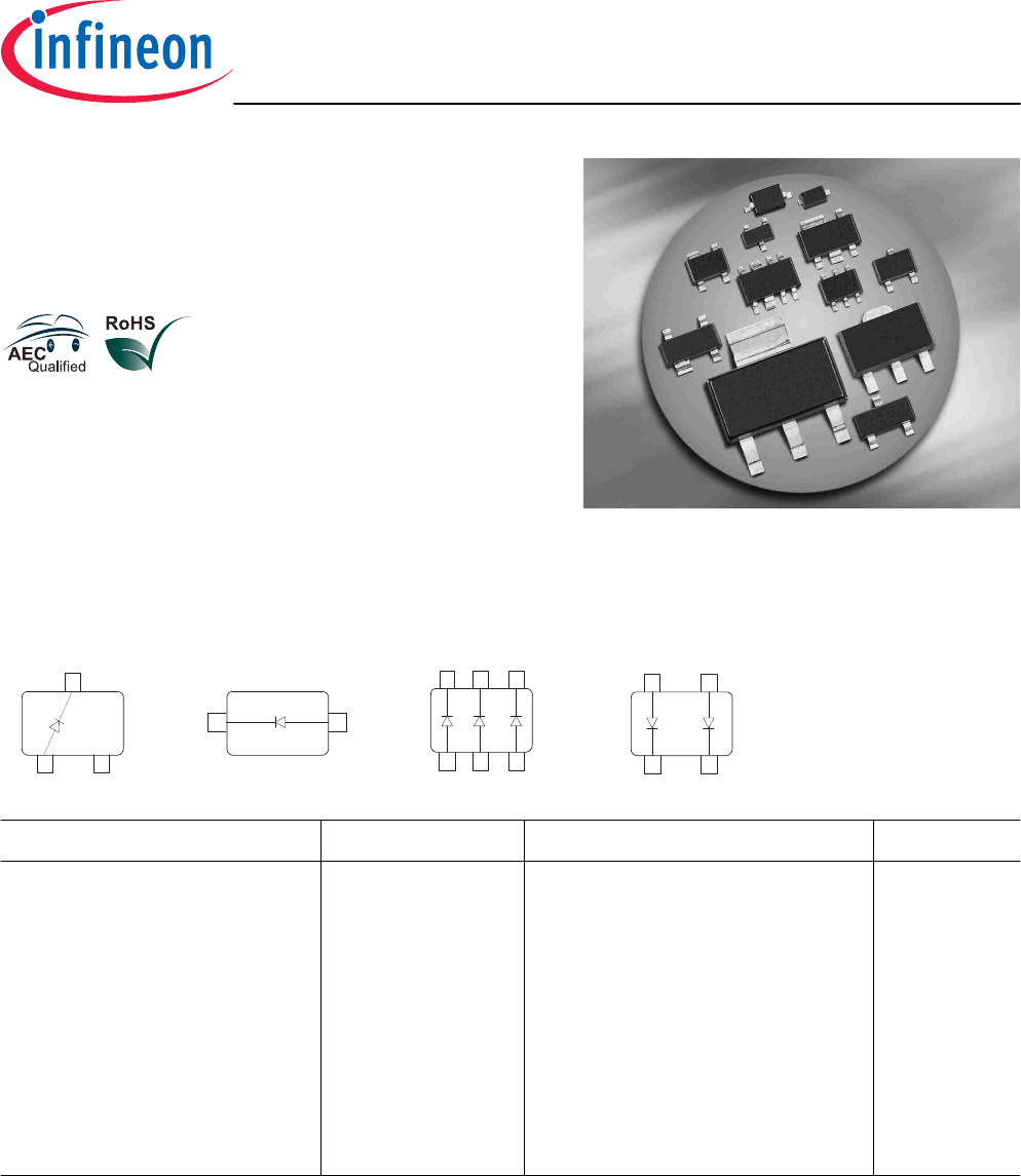
BAS16...
BAS16... Maximum Ratings at TA = 25 °C, unless otherwise specified Parameter Symbol Diode reverse voltage VR 80 Peak reverse voltage VRM 85 Forward current IF Value 250 BAS16-02L, -07L4 200 BAS16-02V, -02W 200 BAS16-03W 250 BAS16S 200 BAS16U 200 BAS16W 250 A IFSM t = 1 µs, BAS16/ S/ U/ W/ -03W 4.5 t = 1 µs, BAS16-02L/ -02V/ -02W/ -07L4 2.5 t=1s 0.
BAS16... Thermal Resistance Parameter Symbol Junction - soldering point 1) RthJS Value Unit K/W BAS16, BAS16S ≤ 260 BAS16-02L, -07L4 ≤ 80 BAS16-02V, -02W ≤ 120 BAS16-03W ≤ 135 BAS16U ≤ 150 BAS16W ≤ 125 Electrical Characteristics at TA = 25°C, unless otherwise specified Symbol Values Unit Parameter min. typ. max.
BAS16... Electrical Characteristics at TA = 25°C, unless otherwise specified Symbol Values Unit Parameter min. typ. max. AC Characteristics 2 pF Diode capacitance CT VR = 0 V, f = 1 MHz Reverse recovery time trr - - 4 ns IF = 10 mA, IR = 10 mA, measured at IR = 1mA , RL = 100 Ω Test circuit for reverse recovery time Pulse generator: tp = 100ns, D = 0.05, tr = 0.6ns, R i = 50Ω D.U.T. ΙF Oscillograph Oscillograph: R = 50Ω, tr = 0.35ns, C = 0.
BAS16... Reverse current IR = ƒ (TA) Forward Voltage VF = ƒ (TA) IF = Parameter VR = Parameter 10 5 BAS 16 1.0 EHB00025 nA VF V Ι F = 100 mA 10 4 IR 10 mA 10 3 1 mA 0.5 0.1 mA 70 V 25 V 10 2 10 1 0 25 50 75 100 °C 0 150 0 TA 50 100 Forward current IF = ƒ (VF) Forward current IF = ƒ (T S) TA = 25°C BAS16 150 BAS 16 C TA 150 300 EHB00023 Ι F mA mA 200 IF 100 typ 150 max 100 50 50 0 0 0.5 1.0 V 0 0 1.
BAS16...
BAS16... Forward current IF = ƒ (T S) Forward current IF = ƒ (T S) BAS16U BAS16W 250 300 mA mA 200 200 IF IF 175 150 125 150 100 100 75 50 50 25 0 0 15 30 45 60 90 105 120 °C 75 0 0 150 15 30 45 60 90 105 120 °C 75 TS 150 TS Permissible Puls Load RthJS = ƒ (tp) Permissible Pulse Load BAS16 IFmax / I FDC = ƒ (t p) BAS16 10 3 10 2 IFmax/IFDC K/W RthJS 10 2 0.5 0.2 0.1 0.05 0.02 0.01 0.005 D=0 10 1 10 0 10 -1 -7 10 10 -6 10 -5 10 -4 10 D=0 0.005 0.01 0.
BAS16... Permissible Puls Load RthJS = ƒ (tp) Permissible Pulse Load BAS16-02L, -07L4 IFmax / I FDC = ƒ (t p) BAS16-02L, -07L4 10 2 I Fmax/ I FDC 10 2 RthJS K/W 0.5 0.2 0.1 0.05 0.02 0.01 0.005 D=0 10 1 10 0 -6 10 10 -5 10 -4 10 -3 - D=0 0.005 0.01 0.02 0.05 0.1 0.2 0.
BAS16... Permissible Puls Load RthJS = ƒ (tp) Permissible Pulse Load BAS16-03W IFmax / I FDC = ƒ (t p) BAS16-03W 10 10 2 3 I Fmax/ IFDC RthJS K/W 10 2 D=0 0.005 0.01 0.02 0.05 0.1 0.2 0.5 10 1 D=0.5 0.2 0.1 0.05 0.02 0.01 0.
BAS16... Permissible Puls Load RthJS = ƒ (tp) Permissible Pulse Load BAS16U IFmax / I FDC = ƒ (t p) BAS16U 10 10 2 3 I Fmax/ IFDC RthJS K/W 10 2 D=0 0.005 0.01 0.02 0.05 0.1 0.2 0.5 10 1 D=0.5 0.2 0.1 0.05 0.02 0.01 0.
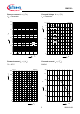
Package SC74 BAS16... Package Outline B 1.1 MAX. 1 2 3 0.35 +0.1 -0.05 Pin 1 marking 0.2 B 6x M A 0.1 MAX. 0.95 0.2 1.9 1.6 ±0.1 4 10˚ MAX. 5 2.5 ±0.1 6 0.25 ±0.1 0.15 +0.1 -0.06 (0.35) 10˚ MAX. 2.9 ±0.2 (2.25) M A Foot Print 2.9 1.9 0.5 0.95 Marking Layout (Example) Small variations in positioning of Date code, Type code and Manufacture are possible.
Package SC79 BAS16... Package Outline 0.2 M A +0.05 0.13 -0.03 0.8 ±0.1 0.2 ±0.05 10˚MAX. 1.6 ±0.1 1 0.3 ±0.05 Cathode marking 10˚MAX. 1.2 ±0.1 A 2 0.55 ±0.04 0.35 1.35 Foot Print 0.35 Marking Layout (Example) 2005, June Date code BAR63-02V Type code Cathode marking Laser marking Standard Packing Reel ø180 mm = 3.000 Pieces/Reel Reel ø180 mm = 8.000 Pieces/Reel (2 mm Pitch) Reel ø330 mm = 10.000 Pieces/Reel Cathode marking 0.4 0.93 0.2 8 1.96 Reel with 2 mm Pitch 2 1.
Package SCD80 BAS16... Package Outline 0.2 M A +0.05 0.13 -0.03 0.8 ±0.1 0.2 ±0.05 10˚MAX. 1.7 ±0.1 1 0.3 ±0.05 Cathode marking 7˚ ±1.5˚ 1.3 ±0.1 A 2 0.7 ±0.1 0.35 1.45 Foot Print 0.35 Marking Layout (Example) 2005, June Date code BAR63-02W Type code Cathode marking Laser marking Standard Packing Reel ø180 mm = 3.000 Pieces/Reel Reel ø180 mm = 8.000 Pieces/Reel (2 mm Pitch) Reel ø330 mm = 10.000 Pieces/Reel Reel with 2 mm Pitch 2 0.2 2.5 8 1.45 Standard 4 Cathode marking 0.4 0.
BAS16...
Package SOD323 15 BAS16...
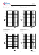
Package SOT23 BAS16... 0.4 +0.1 -0.05 1) 2 0.08...0.1 C 0.95 1.3 ±0.1 1 2.4 ±0.15 3 0.1 MAX. 10˚ MAX. B 1 ±0.1 10˚ MAX. 2.9 ±0.1 0.15 MIN. Package Outline A 5 0...8˚ 1.9 0.2 0.25 M B C M A 1) Lead width can be 0.6 max. in dambar area Foot Print 0.8 0.9 1.3 0.9 0.8 1.2 Marking Layout (Example) Manufacturer EH s 2005, June Date code (YM) Pin 1 BCW66 Type code Standard Packing Reel ø180 mm = 3.000 Pieces/Reel Reel ø330 mm = 10.000 Pieces/Reel 4 0.2 8 2.13 2.65 0.
Package SOT323 BAS16... Package Outline 0.9 ±0.1 2 ±0.2 0.3 +0.1 -0.05 0.1 MAX. 3x 0.1 M 0.1 A 1 2 1.25 ±0.1 0.1 MIN. 2.1 ±0.1 3 0.15 +0.1 -0.05 0.65 0.65 0.2 M A Foot Print 0.8 1.6 0.6 0.65 0.65 Marking Layout (Example) Manufacturer 2005, June Date code (YM) BCR108W Type code Pin 1 Standard Packing Reel ø180 mm = 3.000 Pieces/Reel Reel ø330 mm = 10.000 Pieces/Reel 0.2 2.3 8 4 Pin 1 2.15 1.
Package SOT363 BAS16... Package Outline 2 ±0.2 0.9 ±0.1 +0.1 6x 0.2 -0.05 0.1 0.1 MAX. M 0.1 Pin 1 marking 1 2 3 A 1.25 ±0.1 4 0.1 MIN. 5 2.1 ±0.1 6 0.15 +0.1 -0.05 0.65 0.65 0.2 M A Foot Print 1.6 0.9 0.7 0.3 0.65 0.65 Marking Layout (Example) Small variations in positioning of Date code, Type code and Manufacture are possible. Manufacturer 2005, June Date code (Year/Month) Pin 1 marking Laser marking BCR108S Type code Standard Packing Reel ø180 mm = 3.
Package TSLP-2-1 BAS16... Package Outline Top view Bottom view 0.4 +0.1 0.6 ±0.05 0.05 MAX. 1 1) 1) 0.5 ±0.035 Cathode marking 0.25 ±0.035 2 1 1 ±0.05 0.65±0.05 2 1) Dimension applies to plated terminal Foot Print 0.6 0.275 For board assembly information please refer to Infineon website "Packages" Copper Solder mask 0.375 0.275 0.35 1 0.3 0.925 0.35 0.
Package TSLP-4-4 20 BAS16...
BAS16... Edition 2006-02-01 Published by Infineon Technologies AG 81726 München, Germany © Infineon Technologies AG 2007. All Rights Reserved. Attention please! The information given in this dokument shall in no event be regarded as a guarantee of conditions or characteristics (“Beschaffenheitsgarantie”).