BC857...-BC860... PNP Silicon AF Transistor • For AF input stages and driver applications • High current gain • Low collector-emitter saturation voltage • Low noise between 30 hz and 15 kHz • Complementary types: BC847...-BC850...
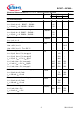
BC857...-BC860... Maximum Ratings Parameter Symbol Collector-emitter voltage VCEO Value V BC857..., BC860... 45 BC858..., BC859... 30 Collector-base voltage Unit VCBO BC857..., BC860... 50 BC858..., BC859...
BC857...-BC860... Electrical Characteristics at TA = 25°C, unless otherwise specified Parameter Symbol Values min. typ. max. DC Characteristics Collector-emitter breakdown voltage V(BR)CEO IC = 10 mA, IB = 0 , BC857..., BC860... 45 - - IC = 10 mA, IB = 0 , BC858..., BC859... 30 - - IC = 10 µA, IE = 0 , BC857..., BC860... 50 - - IC = 10 µA, IE = 0 , BC858..., BC859...
BC857...-BC860... Electrical Characteristics at TA = 25°C, unless otherwise specified Symbol Parameter Values Unit min. typ. max. fT - 250 - MHz Ccb - 1.5 - pF Ceb - 8 - AC Characteristics Transition frequency IC = 20 mA, VCE = 5 V, f = 100 MHz Collector-base capacitance VCB = 10 V, f = 1 MHz Emitter-base capacitance VEB = 0.5 V, f = 1 MHz Short-circuit input impedance kΩ h11e IC = 2 mA, VCE = 5 V, f = 1 kHz, h FE-grp.A - 2.7 - IC = 2 mA, VCE = 5 V, f = 1 kHz, h FE-grp.
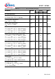
BC857...-BC860... DC current gain hFE = ƒ(IC) VCE = 1 V Collector-emitter saturation voltage IC = ƒ(VCEsat ), hFE = 20 EHP00382 10 3 h FE 5 EHP00380 10 2 mA ΙC 100 C 100 C 25 C -50 C 25 C -50 C 10 2 10 1 5 5 10 1 10 5 5 10 0 10 -2 5 10 -1 5 10 0 5 10 1 mA 10 ΙC 10 -1 2 0 0.1 0.2 0.3 0.4 V 0.
BC857...-BC860...
BC857...-BC860... Total power dissipation P tot = ƒ(TS) Permissible Pulse Load BC857W-BC860W Ptotmax/PtotDC = ƒ(tp ) BC857/W-BC860/W 300 EHP00377 10 3 mW Ptot max 5 Ptot DC 250 D= tp tp T T Ptot 225 10 2 200 175 D= 0 0.005 0.01 0.02 0.05 0.1 0.2 0.
Package SOT23 BC857...-BC860... 0.4 +0.1 -0.05 1) 2 0.08...0.1 C 0.95 1.3 ±0.1 1 2.4 ±0.15 3 0.1 MAX. 10˚ MAX. B 1 ±0.1 10˚ MAX. 2.9 ±0.1 0.15 MIN. Package Outline A 5 0...8˚ 1.9 0.2 0.25 M B C M A 1) Lead width can be 0.6 max. in dambar area Foot Print 0.8 0.9 1.3 0.9 0.8 1.2 Marking Layout (Example) Manufacturer EH s 2005, June Date code (YM) Pin 1 BCW66 Type code Standard Packing Reel ø180 mm = 3.000 Pieces/Reel Reel ø330 mm = 10.000 Pieces/Reel 4 0.2 8 2.13 2.
Package SOT323 BC857...-BC860... Package Outline 0.9 ±0.1 2 ±0.2 0.3 +0.1 -0.05 0.1 MAX. 3x 0.1 M 0.1 A 1 2 1.25 ±0.1 0.1 MIN. 2.1 ±0.1 3 0.15 +0.1 -0.05 0.65 0.65 0.2 M A Foot Print 0.8 1.6 0.6 0.65 0.65 Marking Layout (Example) Manufacturer 2005, June Date code (YM) BCR108W Type code Pin 1 Standard Packing Reel ø180 mm = 3.000 Pieces/Reel Reel ø330 mm = 10.000 Pieces/Reel 0.2 2.3 8 4 Pin 1 2.15 1.
Package TSLP-3-1 BC857...-BC860... Package Outline Bottom view 0.4 +0.1 0.6 ±0.05 0.5 ±0.035 2 1 ±0.05 3 0.65 ±0.05 3 1) 2 1 1) 0.05 MAX. 0.35 ±0.05 Pin 1 marking 2 x 0.15 ±0.035 2 x 0.25 ±0.035 1 0.25 ±0.035 1) Top view 1) 1) Dimension applies to plated terminal Foot Print R0.1 0.2 0.225 0.2 0.225 0.315 0.35 1 0.3 0.945 0.35 0.45 0.275 0.6 0.355 For board assembly information please refer to Infineon website "Packages" 0.17 0.
BC857...-BC860... Edition 2009-11-16 Published by Infineon Technologies AG 81726 Munich, Germany 2009 Infineon Technologies AG All Rights Reserved. Legal Disclaimer The information given in this document shall in no event be regarded as a guarantee of conditions or characteristics.