Data Sheet, Rev. 2.4, Aug.
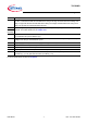
TLE6288R Table of Contents Table of Contents Table of Contents . . . . . . . . . . . . . . . . . . . . . . . . . . . . . . . . . . . . . . . . . . . . . . . . . . . . . . . . . . . . . . . . 2 1 Block Diagram . . . . . . . . . . . . . . . . . . . . . . . . . . . . . . . . . . . . . . . . . . . . . . . . . . . . . . . . . . . . . . . . . . . 4 2 2.1 2.2 2.3 Pin Configuration . . . . . . . . . . . . . . . . . . . . . . . . . . . . . . . . . . . . . . . . . . . . . . . . . . . . . . . . . . . . . . . .
TLE6288R Features • • • • • • • 3 Channel high side with adjustable Peak & Hold current control 3 Channel high/low side configurable Protection – Overcurrent (current limitation) – Overtemperature – Overvoltage (active clamping) Diagnosis – Overcurrent – Overtemperature – Open load (Off-State) – Short to Ground (Off-state, lowside configuration) – Short to VB (Off-state, highside configuration) • Electrostatic discharge (ESD) protection of all pins Interface and Control • Green Product (RoHS compliant)
TLE6288R Block Diagram 1 Block Diagram Reset VDO DOUT 3 / VB VCC Vcc VB . Fault Channel 3 Highside 300 m Ω Peak&Hold . . . . . . . CLKProg IN 1 IN 2 IN 3 IN 4 IN 5 IN 6 Logic Driver Diagnosis DIAG 1 SOUT 3 Channel 2 Highside 300 m Ω Peak&Hold DOUT 2 Channel 1 Highside 300 m Ω Peak&Hold DOUT 1 Channel 4 Highside/ Lowside 300 mΩ DOUT 4 Channel 5 Highside/ Lowside 300 mΩ DOUT 5 Channel 6 Highside/ Lowside 300 mΩ DOUT 6 SOUT 2 SOUT 1 SOUT 4 SOUT 5 DIAG 5 DIAG 6 Overtemp.
TLE6288R Pin Configuration 2 Pin Configuration 2.1 Pin Assignment Figure 2 Pin Configuration PG-DSO-36-26 2.
TLE6288R Pin Configuration Pin Symbol Function 17 DOUT5 Drain Output CH 5 (high/low side) 18 SOUT5 Source Output CH 5 (high/low side) 19 SOUT3 Source Output CH 3 (high side) 20 DOUT3 Drain Output CH 3 (high side) 21 VCP Charge Pump capacitor pin 22 FSIN All Channels Enable/Disable 23 GND Logic Ground 24 Fault General Fault Flag 25 IN3 Control Input Channel 3 26 IN6 Control Input Channel 6 27 Reset Reset pin (+ Standby Mode) 28 Logic Supply Voltage (5 V) 29 VCC VDO 30
TLE6288R Pin Configuration Symbol Description CLKProg Programming pin for the SPI Clock signal. This pin can be used to configure the clock signal input of the SPI. In low state the SPI will read data at the rising clock edge and write data at the falling clock edge. In high state the SPI will read data at the falling clock edge and write data at the rising clock edge. The pin has an internal pull-down structure.
TLE6288R General Product Characteristics 3 General Product Characteristics 3.1 Absolute Maximum Ratings Absolute Maximum Ratings 1) Tj = -40 °C to +150 °C; all voltages with respect to ground, positive current flowing into pin (unless otherwise specified) Pos. Parameter Symbol Limit Values Unit PIN / Conditions Min. Max. VB VB VB VCC VDO VDSL -0.3 – – 20 24 40 V DOUT1-3 DOUT1-32) DOUT1-32) -0.
TLE6288R General Product Characteristics Attention: Integrated protection functions are designed to prevent IC destruction under fault conditions described in the data sheet. Fault conditions are considered as “outside” normal operating range. Protection functions are not designed for continuous repetitive operation. 40V 10 times (once/ 30sec) 12V 160ms 350ms Figure 3 Test Condition 3.2 Thermal Resistance Pos. Parameter Symbol Limit Values Min. Typ. Unit Max. 3.2.1 3.2.2 3.2.
TLE6288R Description 4 Description 4.
TLE6288R Description 4.1.2 • • • Current Regulator: Peak Current Control with Fixed Off-Time Hold only: When the channel is turned on externally (SPI or parallel input) the current rises to the programmed hold current level. Then the channel is internally turned off and a timer is started for a fixed off-time (e.g. 200 µs). After this time the channel is internally turned on again until the hold current level is reached again and so on.
TLE6288R Description Input Signal No Regulation Current defined only by load Ihd Hold only tfo Ipk Ihd Peak & Hold with min. peak time tfo Ipk tfo Ihd Peak and Hold with set peak time Figure 6 Data Sheet tfo tp Current Forms of the Different Current Control Modes of Channel 1-3 12 Rev. 2.
TLE6288R Description 4.2 Protection The TLE6288R has integrated protection functions1) for overload and short circuit (active current limitation), overtemperature, ESD at all pins and overvoltage at the power outputs (zener clamping). Overtemperature Behavior Each channel has an overtemperature sensor and is individually protected against overtemperature. As soon as overtemperature occurs the channel is immediately turned off.
TLE6288R Description 4.3 Diagnostic The TLE6288R has a parallel diagnosis via 6 output pind (DIAG1 - DIAG6) and a serial diagnosis functionallity via SPI. 4.3.1 Parallel Diagnostic Functions Parallel diagnostic pins (push-pull) change state according to the input signal of the corresponding channel. As soon as an error occurs at the corresponding channel (overload and overtemperature is detected in on state and open load/switch bypass in off state) the DIAG output shows the inverted input signal.
TLE6288R SPI 5 SPI The SPI is a Serial Peripheral Interface with 4 digital pins and a 16-bit shift register. The SPI is used to configure and program the device, turn on and off channels and to read detailed diagnostic information. CS SCLK SI SO Figure 7 Serial Peripheral Interface 5.1 SPI Signal Description SPI CS - Chip Select. The system microcontroller selects the TLE6288R by means of the CS pin.
TLE6288R SPI edge (if CLKProg = L; rising edge if CLKProg = H) of serial clock. It is essential that the SCLK pin is in a logic high state (if CLKProg = L; low state if CLKProg = H) whenever chip select CS makes any transition. SI - Serial Input. Serial data bits are shifted in at this pin, the most significant bit (MSB) first. SI information is read in on the rising edge of SCLK (if CLKProg = L; falling edge if CLKProg = H).
TLE6288R SPI Electrical Characteristics: SPI Timing (cont’d) VCC = 4.5 V to 5.5 V, Tj = -40 °C to +150 °C, VB = 6 V to 16 V, Reset = H, VDO = VCC, all voltages with respect to ground, positive current flowing into pin (unless otherwise specified) Pos. Parameter Symbol 2) 5.2.10 Transfer Delay Time (CS high time between two accesses) tdt 5.2.11 Data Valid Time1) CL = 50 pF to 100 pF CL = 220 pF tvalid Limit Values Min. Typ. Max.
TLE6288R SPI Normal function: The bit combination HH indicates that there is no fault condition, i.e. normal function. Overload, Shorted Load or Overtemperature: HL is set when the current limitation gets active, i.e. there is a overload, short to supply or overtemperature condition. The second reason for this bit combination is overtemperature of the corresponding channel.
TLE6288R SPI The following parameters and functional behavior can be programmed by SPI: • • • • • • • • • • Current regulation mode (mode): for each of the 3 highside channels individually the operation mode can be set.
TLE6288R SPI Legend of SPI Command Table • • • • • • • • • • • Mode: Operation mode of the current regulator: – no regulation – hold only – peak & hold with minimum peak time – peak & hold with programmed peak time Ipk: Peak current values 1.2 A … 3.6 A Ihd: Hold current values 0.7 A … 2 A tp: Peak time value 0.8 ms … 3.
TLE6288R SPI 5.6 Bit Assignment and Default Settings for Internal Logic Registers Mode 00 no current regulation 01 hold only 10 P&H minimum peak time 11 P&H with programmed times Peak Current (Ipk) 1.2 A 1.8 A 2.4 A 3.6 A 2 Bits 00 01 10 11 Hold Current (Ihd) 0.7 A 1.0 A 1.4 A 2.0 A 2 Bits 00 01 10 11 Fixed off Time (tfo) 100 µs 200 µs 300 µs 400 µs 2 Bits 00 01 10 11 Peak Time (tp) 0.8 ms 1.2 ms 1.6 ms 2.0 ms 2.4 ms 2.8 ms 3.2 ms 3.
TLE6288R SPI 5.7 SPI Timing Diagrams CS 0.7Vcc tdt 0.2 Vcc tlagL tSCKH 0.7Vcc SCLK tleadL tSUL 0.2Vcc tSCKL tHL 0.7Vcc SI 0.2Vcc Figure 11 Input Timing Diagram (CLKProg = L) CS 0.2 Vcc SCLK 0.2 Vcc tvalid tDis 0.7 Vcc SO SO 0.2 Vcc SO 0.7 Vcc 0.
TLE6288R SPI CS 0.7Vcc tdt 0.2 Vcc tlagH tSCKH tleadH 0.7Vcc 0.2Vcc SCLK tSCKL tSUH tHH 0.7Vcc SI 0.2Vcc Figure 14 Input Timing Diagram (CLKProg = H) 0.7 V cc CS SCLK 0.2 V cc t valid t Dis 0.7 V cc SO SO 0.2 V cc SO 0.7 V cc 0.
TLE6288R Electrical Characteristics Input / Output Pins 6 Electrical Characteristics Input / Output Pins 6.1 Power Supply, Reset Electrical Characteristics: Power Supply, Reset VCC = 4.5 V to 5.5 V, Tj = -40 °C to +150 °C, VB = 6 V to 16 V, Reset = H, VDO = VCC, all voltages with respect to ground, positive current flowing into pin (unless otherwise specified) Pos. Parameter Symbol Min. Typ. Max. 6.1.1 Power Supply Current 1 – – 6.1.2 Power Supply Current 2 – 6.1.
TLE6288R Electrical Characteristics Input / Output Pins Electrical Characteristics: Power Outputs (cont’d) VCC = 4.5 V to 5.5 V, Tj = -40 °C to +150 °C, VB = 6 V to 16 V, Reset = H, VDO = VCC, all voltages with respect to ground, positive current flowing into pin (unless otherwise specified) Pos. Parameter Symbol Limit Values Min. Typ. Max. Unit Pin/ Conditions Comment 6.2.14 Output OFF Delay time tdOFF – – 20 µs – HS- Mode LS- Mode see Figure 17 6.2.
TLE6288R Electrical Characteristics Input / Output Pins Electrical Characteristics: Digital Inputs (cont’d) VCC = 4.5 V to 5.5 V, Tj = -40 °C to +150 °C, VB = 6 V to 16 V, Reset = H, VDO = VCC, all voltages with respect to ground, positive current flowing into pin (unless otherwise specified) Pos. Parameter Symbol Limit Values Min. Typ. Max. Unit Pin/ Conditions Comment 6.3.6 SPI Input pull-down current Ipd 10 20 50 µA SI, SCLK VIN = 5 V (CLKProg = H) 6.3.
TLE6288R Application Information 7 Application Information 7.1 Zthjc Diagram Junction - Case for Single channel operation Zth(D, Pulse width) [K/W] 10 1 Dutycycle D 0,1 0,5 0,2 0,1 0,05 0,02 0,01 0,01 0,000001 0,00001 0,0001 0,001 0,01 0,1 Pulse width [s] Figure 18 • Zthjc Diagram Conditions for Figure 18 – Results based on FEM Simulations – Tcase = 125 °C – Single Channel operation, 0.8W power dissipation 7.
TLE6288R Application Information Figure 19 FE Model of the JEDEC 2s2p PCB Figure 20 Thermal via layout Figure 19 showes the Product TLE6288R on the 2s2p board used to specify the typical RthjA value in Chapter 3.2. In Figure 20, the thermal via layout according to JESD51-5 is shown. Data Sheet 28 Rev. 2.
TLE6288R Application Information 7.3 Overload/Low Inductance Load Detection in Current Regulation Mode Input Signal Ipk / Ihd Load Current normal condition tli tfo Overload / low inductance load detection Ipk / Ihd Load Current low-inductance load tli tfo Figure 21 Data Sheet 29 Rev. 2.
TLE6288R Package Outlines Package Outlines 0.65 0.25 +0.13 6.3 0.1 C (Mold) 5˚ ±3˚ 0.25 2.8 1.3 15.74 ±0.1 (Heatslug) B +0.07 -0.02 11 ±0.15 1) 3.5 MAX. 0 +0.1 1.1 ±0.1 3.25 ±0.1 8 Heatslug 0.95 ±0.15 36x 0.25 M A B C 14.2 ±0.3 0.25 B 19 1 18 10 36 5.9 ±0.1 (Metal) 19 3.2 ±0.1 (Metal) Bottom View 36 Index Marking 1 x 45˚ 15.9 ±0.1 1) (Mold) 1) A 13.7 -0.2 (Metal) 1 Heatslug Does not include plastic or metal protrusion of 0.15 max.
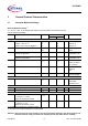
TLE6288R Revision History 9 Revision Revision History Date Changes 2.2 2004-03-25 Preliminary Datasheet TLE6288R Vp2.2 2.3 2006-05-03 Formal changes, Thermal information added, Spec. values not changed 2.
Edition 2007-08-08 Published by Infineon Technologies AG 81726 Munich, Germany © 2007 Infineon Technologies AG All Rights Reserved. Legal Disclaimer The information given in this document shall in no event be regarded as a guarantee of conditions or characteristics.