
Datasheet


TLE6288R
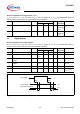
Electrical Characteristics Input / Output Pins
Data Sheet 26 Rev. 2.4, 2007-08-08
6.4 Digital Outputs
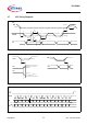
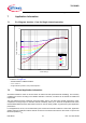
Figure 17 Turn on/off Timings with Resistive Load
6.3.6 SPI Input pull-down current
I
pd
10 20 50 µA SI, SCLK
(CLKProg
= H)
V
IN
= 5 V
6.3.7 SPI Input pull-up current
I
pu
-50 -20 -10 µA CS, SCLK
(CLKProg
= L)
V
IN
= GND
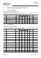
Electrical Characteristics: Digital Outputs
V
CC
= 4.5 V to 5.5 V, T
j
= -40 °C to +150 °C, V
B
= 6 V to 16 V, Reset = H, V
DO
= V
CC
, all voltages with respect to
ground, positive current flowing into pin (unless otherwise specified)
Pos. Parameter Symbol Limit Values Unit Pin/
Comment
Conditions
Min. Typ. Max.
6.4.1 SO Low State Output Voltage
V
SOL
––0.4VSO I
SOL
= 2.5 mA
6.4.2 SO High State Output Voltage
V
SOH
V
DO
-
0.4 V
––VSO I
SOH
= -2 mA
6.4.3 DIAG Low State Output
Voltage
V
DIAGL
– – 0.4 V DIAG1-6 I
DIAGL
= 50 µA
6.4.4 DIAG High State Output
Voltage
V
DIAGH
V
DO
-
0.4 V
––VDIAG1-6I
DIAGH
=
-50 µA
6.4.5 Fault Low Output Voltage
V
ol
––0.4VFaultI
out
= 1 mA
6.4.6 Fault Output leak Current
I
oh
––1µA Fault Output: OFF
V
(fault)
= 5 V
Electrical Characteristics: Digital Inputs (cont’d)
V
CC
= 4.5 V to 5.5 V, T
j
= -40 °C to +150 °C, V
B
= 6 V to 16 V, Reset = H, V
DO
= V
CC
, all voltages with respect to
ground, positive current flowing into pin (unless otherwise specified)
Pos. Parameter Symbol Limit Values Unit Pin/
Comment
Conditions
Min. Typ. Max.
Input Voltage
Output Voltage
(Highside configuration)
70%
30%
t
dON
t
dOFF
t
r
t
f