
Datasheet


Data Sheet 7 Rev. 2.4, 2007-08-08
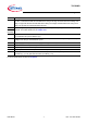
TLE6288R
Pin Configuration
For more details about the SPI see Chapter 5.
CLKProg Programming pin for the SPI Clock signal. This pin can be used to configure the clock signal input of
the SPI. In low state the SPI will read data at the rising clock edge and write data at the falling clock
edge. In high state the SPI will read data at the falling clock edge and write data at the rising clock
edge. The pin has an internal pull-down structure.
DIAG1-5 Parallel diagnostic pins (push-pull) change state according to the input signal of the corresponding
channel. For further details refer to Chapter 4.3.1
DIAG6/
Overtemp
VCP Pin to connect the external capacitor of the integrated charge pump. Connect a ceramic capacitor with
47 nF between this pin and DOUT3 (
V
B
).
V
DO
Supply pin of the push-pull digital output drivers. This pin can be used to vary the high-state output
voltage of the SO pin and the DIAG1-6 pins.
V
CC
Logic supply pin. This pin is used to supply the integrated circuitry.
CS Chip Select of the SPI (active low)
SO Signal Output of the Serial Peripheral Interface
SI Signal Input of the Serial Peripheral Interface. The pin has an internal pull-down structure.
SCLK Clock Input of the Serial Peripheral Interface. The pin has an internal pull-up structure
(if CLKProg = L) or an pull-down structure (if CLKProg = H).
Symbol Description