IFX1050G High Speed CAN-Transceiver Data Sheet Rev. 1.
IFX1050G Table of Contents Table of Contents 1 Overview . . . . . . . . . . . . . . . . . . . . . . . . . . . . . . . . . . . . . . . . . . . . . . . . . . . . . . . . . . . . . . . . . . . . . . . 3 2 Block Diagram . . . . . . . . . . . . . . . . . . . . . . . . . . . . . . . . . . . . . . . . . . . . . . . . . . . . . . . . . . . . . . . . . . . 4 3 3.1 3.2 Pin Configuration . . . . . . . . . . . . . . . . . . . . . . . . . . . . . . . . . . . . . . . . . . . . . . . . . . . . . . . . . . . . . . .
High Speed CAN-Transceiver 1 IFX1050G Overview Features • • • • • • • • CAN data transmission rates from 1 kBaud up to 1 MBaud Receive - Only Mode and Stand - By Mode Optimized Electromagnetic Compatibility (EMC) Optimized for a high immunity against Electromagnetic Interference (EMI) Bus pins are short circuit proof Over - temperature protection Very wide temperature range (-40 °C up to 125 °C) Green Product (RoHS compliant) PG-DSO-8 Description The IFX1050G is optimized for high speed differential
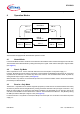
IFX1050G Block Diagram 2 Block Diagram &$1+ &$1/ 9&& 'ULYHU 2XWSXW 6WDJH 7HPS 3URWHFWLRQ 0RGH &RQWURO 7[' ,1+ 50 5HFHLYHU *1' Figure 1 Data Sheet 5[' Block Diagram 4 Rev. 1.
IFX1050G Pin Configuration 3 Pin Configuration 3.1 Pin Assignment 7[' ,1+ *1' &$1+ 9&& &$1/ 5[' 50 3,1&21),*B,); 69* Figure 2 Pin Configuration 3.
IFX1050G Operation Modes 4 Operation Modes INH = 1 Normal Mode INH = 0 RM = 1 INH = 0 and RM = 1 Stand-by Mode INH = 1 RM = 0 / 1 RM = 0 RM = 1 INH = 0 and RM = 0 INH = 1 Receive-only Mode INH = 0 RM = 0 AED02924 Figure 3 Mode State Diagram The IFX1050G is equipped with three different operation modes. 4.1 Normal Mode In the Normal Mode the device is able to receive data from the CAN bus and to transmit messages to the CAN bus.
IFX1050G Electrical Characteristics 5 Electrical Characteristics 5.1 Absolute Maximum Ratings Table 1 Absolute Maximum Ratings Parameter Symbol Limit Values Unit Remarks Min. Max. VCC VCANH/L VI VESD -0.3 6.5 V – -40 40 V – -0.3 VCC V 0 V < VCC < 5.5 V -6 6 kV human body model (100 pF via 1.5 kΩ) VESD -2 2 kV human body model (100 pF via 1.
IFX1050G Electrical Characteristics 6 Electrical Characteristics Table 3 Electrical Characteristics 4.5 V < VCC < 5.5 V; RL = 60 Ω; VINH < VINH,ON; -40 °C < Tj < 125 °C; all voltages with respect to ground; positive current flowing into pin; unless otherwise specified. Parameter Symbol Limit Values Min. Typ. Max.
IFX1050G Electrical Characteristics Table 3 Electrical Characteristics (cont’d) 4.5 V < VCC < 5.5 V; RL = 60 Ω; VINH < VINH,ON; -40 °C < Tj < 125 °C; all voltages with respect to ground; positive current flowing into pin; unless otherwise specified. Parameter Symbol Limit Values Min. Typ. Max. Unit Remarks Bus Receiver Differential receiver threshold voltage, recessive to dominant edge Vdiff,d – 0.75 0.
IFX1050G Electrical Characteristics Table 3 Electrical Characteristics (cont’d) 4.5 V < VCC < 5.5 V; RL = 60 Ω; VINH < VINH,ON; -40 °C < Tj < 125 °C; all voltages with respect to ground; positive current flowing into pin; unless otherwise specified. Parameter Symbol Limit Values Min. Typ. Max.
IFX1050G Electrical Characteristics INH 7 CANH TxD RM 47 pF 8 1 5 60 Ω RxD 6 4 20 pF CANL GND VCC 3 5V 100 nF 2 AEA03328.VSD Figure 4 Test Circuit for Dynamic Characteristics VTxD VCC(33V) GND VDIFF td(L), T td(H), T t VDIFF(d) VDIFF(r) VRxD td(L), R t td(H), R VCC(33V) 0.7VCC(33V) 0.3VCC(33V) GND td(L), TR td(H), TR t AET02926 Figure 5 Data Sheet Timing Diagrams for Dynamic Characteristics 11 Rev. 1.
IFX1050G Application Information 7 Application Information Note: The following information is given as a hint for the implementation of the device only and shall not be regarded as a description or warranty of a certain functionality, condition or quality of the device. 120 Ω IFX1050 VBat CAN Bus RM INH 7 6 RxD CANH TxD CANL 1) VCC GND 5 8 4 µP 1 3 100 nF 2 100 nF GND ESD24VS2B e. g.
IFX1050G Package Outlines 8 Package Outlines 0.1 2) 0.41+0.1 -0.06 0.2 8 5 1 4 5 -0.2 1) M B 0.19 +0.06 C 8 MAX. 1.27 4 -0.21) 1.75 MAX. 0.175 ±0.07 (1.45) 0.35 x 45˚ 0.64 ±0.25 6 ±0.2 A B 8x 0.2 M C 8x A Index Marking 1) Does not include plastic or metal protrusion of 0.15 max. per side 2) Lead width can be 0.61 max.
IFX1050G Revision History 9 Revision History Revision Date Changes 1.0 2009-05-12 Initial data sheet Data Sheet 14 Rev. 1.
Edition 2009-05-14 Published by Infineon Technologies AG 81726 Munich, Germany © 2009 Infineon Technologies AG All Rights Reserved. Legal Disclaimer The information given in this document shall in no event be regarded as a guarantee of conditions or characteristics.