
Datasheet


Data Sheet 4 Rev. 1.01, 2009-10-19
IFX27001
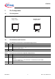
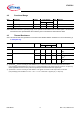
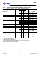
Pin Configuration
3 Pin Configuration
3.1 Pin Assignment
Figure 3 Pin Configuration (top view)
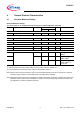
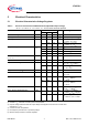
3.2 Pin Definitions and Functions
Table 1 Pin Definitions and Functions Fixed Output Voltage Versions
Pin No. Symbol Function
1GNDGround
2, Tab Q Output; Connect a capacitor C
Q
≥ 10 µF with ESR ≤ 10 Ω between pin Q and GND
Connect to heatsink area.
3I Input
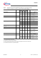
Table 2 Pin Definitions and Functions Adjustable Output Version
Pin No. Symbol Function
1ADJAdjust; defines output voltage by external voltage divider between Q, ADJ and GND.
2, Tab Q Output; the output voltage is defined by the external voltage divider between Q, Adjust and
Ground.
Connect a capacitor C
Q
≥ 10 µF with ESR ≤ 10 Ω between pin Q and GND
Connect to heatsink area.
3I Input
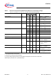
AEP02817
GND
1
Q
I
Q
AEP02821
ADJ
1
Q
I
Q
Fixed Output
Voltage Version
Adjustable Output
Voltage Version