
Datasheet


IFX27001
General Product Characteristics
Data Sheet 5 Rev. 1.01, 2009-10-19
4 General Product Characteristics
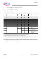
4.1 Absolute Maximum Ratings
Note: Stresses above the ones listed here may cause permanent damage to the device. Exposure to absolute
maximum rating conditions for extended periods may affect device reliability.
Note: Integrated protection functions are designed to prevent IC destruction under fault conditions described in the
data sheet. Fault conditions are considered as “outside” normal operating range. Protection functions are
not designed for continuous repetitive operation.
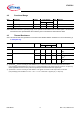
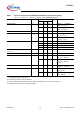
Absolute Maximum Ratings
1)
T
j
= -40 °C to 150 °C; all voltages with respect to ground, (unless otherwise specified)
1) not subject to production test, specified by design
Pos. Parameter Symbol Limit Values Unit Test Condition
Min. Max.
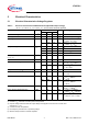
Input I
4.1.1 Voltage
V
I
-0.3 40 V –
Input - Output Voltage Differential (Applies to Adjustable Output Version Only)I
4.1.2 Voltage
V
I
- V
Q
-0.3 40 V –
Output Q
4.1.3 Voltage
V
Q
-0.3 40 V –
Temperature
4.1.4 Junction temperature
T
j
-40 150 °C–
4.1.5 Storage temperature
T
stg
-50 150 °C–
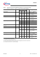
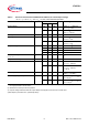
ESD Susceptibility
4.1.6 ESD Absorption
V
ESD,HBM
-2 2 kV Human Body Model
(HBM)
2)
2) ESD susceptibility Human Body Model “HBM” according to AEC-Q100-002 - JESD22-A114
4.1.7 V
ESD,CDM
-500 500 V Charge Device
Model (CDM)
3)
3) ESD susceptibility Charged Device Model “CDM” according to ESDA STM5.3.1
4.1.8 -750 750 V Charge Device
Model (CDM)
3)
at
corner pins