IFX27001 Linear Voltage Regulator IFX27001TFV15 IFX27001TFV18 IFX27001TFV26 IFX27001TFV33 Data Sheet Rev. 1.
Linear Voltage Regulator 1 IFX27001 Overview Features • • • • • • • • 1.5V, 1.8V, 2.6V, 3.3 V, 5.0V or Adj. output voltage 1.0 A output current Low dropout voltage, 1 V (typ.
IFX27001 Block Diagram 2 Block Diagram I Q Control with Overtemperature Protection; Overcurrent Protection Internal Reference GND AES02840 Figure 1 Block Diagram for Fixed Output Voltage (1.5V, 1.8V, 2.6V, 3.3V, 5.0V) I Q Control with Overtemperature Protection; Overcurrent Protection Adjust Internal Reference AES02839 Figure 2 Data Sheet Block Diagram for Adjustable Output Voltage 3 Rev. 1.
IFX27001 Pin Configuration 3 Pin Configuration 3.1 Pin Assignment Fixed Output Voltage Version Adjustable Output Voltage Version Q Q 1 1 Q Q GND I ADJ AEP02817 I AEP02821 Figure 3 Pin Configuration (top view) 3.2 Pin Definitions and Functions Table 1 Pin Definitions and Functions Fixed Output Voltage Versions Pin No. Symbol Function 1 GND Ground 2, Tab Q Output; Connect a capacitor CQ ≥ 10 µF with ESR ≤ 10 Ω between pin Q and GND Connect to heatsink area.
IFX27001 General Product Characteristics 4 General Product Characteristics 4.1 Absolute Maximum Ratings Absolute Maximum Ratings1) Tj = -40 °C to 150 °C; all voltages with respect to ground, (unless otherwise specified) Pos. Parameter Symbol Limit Values Min. Max. -0.3 40 Unit Test Condition V – Input I 4.1.1 Voltage VI Input - Output Voltage Differential (Applies to Adjustable Output Version Only)I 4.1.2 Voltage VI - VQ -0.3 40 V – Voltage VQ -0.
IFX27001 General Product Characteristics 4.2 Pos. Functional Range Parameter 4.2.1 Input voltage 4.2.2 Junction temperature Symbol VI Tj Limit Values Unit Min. Max. VI + VDR 40 V -40 125 °C Remarks – Note: Within the functional or operating range, the IC operates as described in the circuit description. The electrical characteristics are specified within the conditions given in the Electrical Characteristics table. 4.
IFX27001 Electrical Characteristics 5 Electrical Characteristics 5.1 Electrical Characteristics Voltage Regulator Table 3 Electrical Characteristics IFX27001TFV DV (adjustable output voltage) -40 °C < Tj < 125 °C; VI - VQ = 13.5 V, IQ = 10 mA; unless otherwise specified Parameter Reference voltage Line regulation Load regulation Symbol Limit Values min. typ. 1) VREF 1.20 1.25 Δ VQ – 0.5 Δ VQ – 0.2 Unit Measuring Conditions max. 1.30 1.50 0.4 V % 2) % 2) – 0.25 0.5 % 2) 1.00 1.05 1.10 1.
IFX27001 Electrical Characteristics Table 4 Electrical Characteristics IFX27001TFV15 DV15 (1.5 V fixed output voltage) -40 °C < Tj < 125 °C; VI = 13.5 V, IQ = 10 mA; unless otherwise specified Parameter Output voltage Symbol VQ Limit Values Unit Measuring Conditions min. typ. max. 1.45 1.5 1.55 V 10 mA ≤ IQ ≤ 1000 mA; 2.9 V ≤ VI ≤ 16 V – 1.5 – V 10 mA ≤ IQ ≤ 1000 mA; 16 V ≤ VI ≤ 40 V 1) Line regulation ΔVQ – 4.8 22.5 mV 2.9 V ≤ VI ≤ 40 V Load regulation ΔVQ – 2.6 5.
IFX27001 Electrical Characteristics Table 5 Electrical Characteristics IFX27001TFV18 DV18 (1.8 V fixed output voltage) -40 °C < Tj < 125 °C; VI = 13.5 V, IQ = 10 mA; unless otherwise specified Parameter Output voltage Symbol VQ Limit Values Unit Measuring Conditions min. typ. max. 1.75 1.8 1.85 V 10 mA ≤ IQ ≤ 1000 mA; 3.2 V ≤ VI ≤ 16 V – 1.8 – V 10 mA ≤ IQ ≤ 1000 mA; 16 V ≤ VI ≤ 40 V 1) Line regulation ΔVQ – 7.2 27 mV 3.2 V ≤ VI ≤ 40 V Load regulation ΔVQ – 3.4 7.
IFX27001 Electrical Characteristics Table 6 Electrical Characteristics IFX27001TFV26 DV26 (2.6 V fixed output voltage) -40 °C < Tj < 125 °C; VI = 13.5 V, IQ = 10 mA; unless otherwise specified Parameter Output voltage Symbol VQ Limit Values Unit Measuring Conditions min. typ. max. 2.52 2.60 2.68 V 10 mA ≤ IQ ≤ 1000 mA; 4.0 V ≤ VI ≤ 16 V – 2.60 – V 10 mA ≤ IQ ≤ 1000 mA; 16 V ≤ VI ≤ 40 V 1) Line regulation ΔVQ – 11 40 mV 4.
IFX27001 Electrical Characteristics Table 7 Electrical Characteristics IFX27001TFV33 DV33 (3.3 V fixed output voltage) -40 °C < Tj < 125 °C; VI = 13.5 V, IQ = 10 mA; unless otherwise specified Parameter Symbol Output voltage VQ Limit Values Unit Measuring Conditions Min. Typ. Max. 3.20 3.3 3.40 V 10 mA ≤ IQ ≤ 1000 mA; 4.7 V ≤ VI ≤ 16 V – 3.3 – V 10 mA ≤ IQ ≤ 1000 mA ; 16 V ≤ VI ≤ 40 V 1) Line regulation Δ VQ – 15 50 mV 4.
IFX27001 Electrical Characteristics Table 8 Electrical Characteristics IFX27001TFV50 DV50 (5.0 V fixed output voltage) -40 °C < Tj < 125 °C; VI = 13.5 V, IQ = 10 mA; unless otherwise specified Parameter Output voltage Symbol VQ Limit Values Unit Measuring Conditions min. typ. max. 4.85 5.00 5.15 V 10 mA ≤ IQ ≤ 1000 mA; 6.4 V ≤ VI ≤ 16 V – 5.00 – V 10 mA ≤ IQ ≤ 1000 mA; 16V ≤ VI ≤ 40 V 1) Line regulation ΔVQ – 20 75 mV 6.
IFX27001 Electrical Characteristics IFX27001TFV II VI CI I 3 2 Q IQ CQ 100 nF VQ 1 GND IGND IFX27001TFV II VI CI I 3 2 Q IQ CQ 100 nF R1 1 ADJ IADJ VQ R2 Figure 4 Data Sheet Measuring Circuit of fixed output voltage versions and adjustable output voltage version 13 Rev. 1.
IFX27001 Electrical Characteristics 5.2 Typical Performance Characteristics Voltage Regulator Current Consumption Iq versus Junction Temperature TJ Current Consumption Iq versus Input Voltage VI 3_Iq-VI.vsd 1_Iq-Tj.vsd Iq [mA] Iq [mA] VI = 13.5V VI = 13.5V IQ = 10mA IQ = 1mA 10 10 IQ = 10mA IQ = 500mA IQ = 1000mA 1 1 5.0V-Version 3.3V-Version 2.6V-Version 1.8V-Version 1.5V-Version 0.1 0.1 0.01 -40 -20 0 0.
IFX27001 Electrical Characteristics Output Voltage VQ versus Input Voltage VI Power Supply Ripple Rejection versus Frequency 11_VI-VQ.vsd 6.00 Ta= 25 °C VQ [V] VRIPPLE = 0.5 V VIN = 13.5 V CADJ = 10 µF Tantalum Ta = 25 °C PSRR IQ = 100mA 5.0V-Version 13_PSRR.VSD 90 [dB] IQ = 10mA 4.00 70 3.3V-Version 3.00 60 2.6V-Version 1.8V-Version 2.00 50 IQ = 10 mA IQ = 125 mA IQ = 250 mA IQ = 500 mA IQ = 1000 mA 1.5V-Version 1.
IFX27001 Application Information 6 Application Information Note: The following information is given as a hint for the implementation of the device only and shall not be regarded as a description or warranty of a certain functionality, condition or quality of the device.
IFX27001 Application Information For the variable regulator IFX27001TFV, a minimum load current of 5 mA is necessary in order to keep the output voltage regulated. If the application does not assure this minimum load requirement, the output voltage divider should be dimensioned sufficiently low-ohmic: R1 ≤ 240 Ω. For the variable voltage type an additional decoupling a capacitor CADJ at the adjust pin improves the ripple rejection ratios. Placing CADJ requires an increased output capacitance of CQ ≥ 22 µF.
IFX27001 Package Outlines Package Outlines 6.5 +0.15 -0.05 A 0.15 MAX. per side 2.3 +0.05 -0.10 B (5) 3x 0.75 ±0.1 0.5 +0.08 -0.04 2.28 4.57 0.5 +0.08 -0.04 0.9 +0.20 -0.01 0...0.15 0.8 ±0.15 (4.24) 1 ±0.1 9.98 ±0.5 6.22 -0.2 5.4 ±0.1 0.51 MIN. 7 0.1 B 0.25 M A B All metal surfaces tin plated, except area of cut.
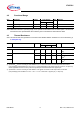
IFX27001 Revision History 8 Revision History Revision Date Changes 1.01 2009-10-19 Coverpage changed Overview page: Inserted reference statement to TLE/TLF series. 1.0 2009-04-28 Initial Release Data Sheet 19 Rev. 1.
Edition 2009-10-19 Published by Infineon Technologies AG 81726 Munich, Germany © 2009 Infineon Technologies AG All Rights Reserved. Legal Disclaimer The information given in this document shall in no event be regarded as a guarantee of conditions or characteristics.