
Datasheet


www.irf.com 1
Parameter Maximum Units
I
D
@ T
A
= 25°C Continuous Drain Current, V
GS
@10V➃ 5.8 A
I
D
@ T
A
= 70°C 4.6
I
DM
Pulsed Drain Current ➀ 46
P
D
@T
A
= 25°C Power Dissipation ➃ 2.0 W
P
D
@T
A
= 70°C 1.3
Linear Derating Factor 16 W/°C
V
GS
Gate-to-Source Voltage ± 20 V
dv/dt Peak Diode Recovery dv/dt ➁ -5.0 V/ns
T
J,
T
STG
Junction and Storage Temperature Range -55 to +150 °C
IRF7421D1
PRELIMINARY
FETKY
MOSFET / Schottky Diode
Notes:
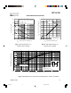
➀ Repetitive rating; pulse width limited by maximum junction temperature (see figure 11)
➁ I
SD
≤ 4.1A, di/dt ≤ 110A/µs, V
DD
≤ V
(BR)DSS
, T
J
≤ 150°C
➂ Pulse width ≤ 300µs; duty cycle ≤ 2%
➃ Surface mounted on FR-4 board, t ≤ 10sec.
Parameter Maximum Units
R
θJA
Junction-to-Ambient ➃ 62.5 °C/W
Absolute Maximum Ratings (T
A
= 25°C unless otherwise noted)
Thermal Resistance Ratings
8/20/98
The FETKY family of co-packaged HEXFETs and Schottky diodes offer
the designer an innovative board space saving solution for switching
regulator applications. Generation 5 HEXFETs utilize advanced processing
techniques to achieve extremely low on-resistance per silicon area. Combining
this technology with International Rectifier's low forward drop Schottky
rectifiers results in an extremely efficient device suitable for use in a wide
variety of portable electronics applications.
The SO-8 has been modified through a customized leadframe for enhanced
thermal characteristics. The SO-8 package is designed for vapor phase,
infrared or wave soldering techniques.
Description
l Co-packaged HEXFET
®
Power
MOSFET and Schottky Diode
l Ideal For Synchronous Regulator
Applications
l Generation V Technology
l SO-8 Footprint
V
DSS
= 30V
R
DS(on)
= 0.035Ω
Schottky Vf = 0.39V
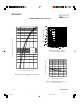
8
1
2
3
4
5
6
7
D
D
D
DG
S
A
S
A
A
Top View
SO-8
TM
PD- 91411C
7421d1.p65 8/20/98, 4:07 PM1