
Datasheet
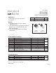
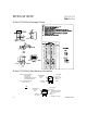

Symbol Parameter Max. Units
V
DS
Drain-Source Voltage 100 V
V
GS
Gate-to-Source Voltage ± 20
I
D
@ T
C
= 25°C Continuous Drain Current, V
GS
@ 10V 31
I
D
@ T
C
= 100°C Continuous Drain Current, V
GS
@ 10V 22 A
I
DM
Pulsed Drain Current 125
P
D
@T
C
= 25°C Maximum Power Dissipation 110 W
P
D
@T
A
= 25°C Maximum Power Dissipation 3.0
Linear Derating Factor 0.71 mW°C
dv/dt Peak Diode Recovery dv/dt 15 V/ns
T
J
Operating Junction and -55 to + 175 °C
T
STG
Storage Temperature Range
Soldering Temperature, for 10 seconds 300 (1.6mm from case )
www.irf.com 1
12/03/04
IRFR3410PbF
IRFU3410PbF
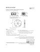
HEXFET
®
Power MOSFET
V
DSS
R
DS(on)
max I
D
100V 39mΩ 31A
Notes through are on page 10
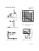
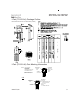
D-Pak
IRFR3410
I-Pak
IRFU3410
PD - 95514A
l High frequency DC-DC converters
l Lead-Free
Benefits
Applications
l Low Gate-to-Drain Charge to Reduce
Switching Losses
l Fully Characterized Capacitance Including
Effective C
OSS
to Simplify Design, (See
App. Note AN1001)
l Fully Characterized Avalanche Voltage
and Current
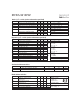
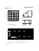
Parameter Typ. Max. Units
R
θJC
Junction-to-Case ––– 1.4
R
θJA
Junction-to-Ambient (PCB mount)* ––– 40 °C/W
R
θJA
Junction-to-Ambient ––– 110
Thermal Resistance
Absolute Maximum Ratings