
Datasheet

IRFR/U3410PbF
www.irf.com 5
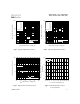
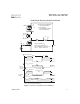
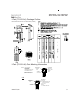
Fig 10a. Switching Time Test Circuit
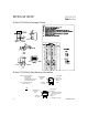
V
DS
9
0%
1
0%
V
GS
t
d(on)
t
r
t
d(off)
t
f
Fig 10b. Switching Time Waveforms
V
DS
Pulse Width ≤ 1 µs
Duty Factor ≤ 0.1 %
R
D
V
GS
R
G
D.U.T.
V
GS
+
-
V
DD
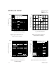
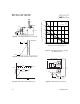
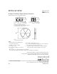
Fig 11. Maximum Effective Transient Thermal Impedance, Junction-to-Case
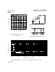
Fig 9. Maximum Drain Current Vs.
Case Temperature
25 50 75 100 125 150 175
T
C
, Case Temperature (°C)
0
4
8
12
16
20
24
28
32
I
D
,
D
r
a
i
n
C
u
r
r
e
n
t
(
A
)
LIMITED BY PACKAGE
1E-006 1E-005 0.0001 0.001 0.01 0. 1
t
1
, Rectangular Pulse Duration (sec)
0.001
0.01
0.1
1
10
T
h
e
r
m
a
l
R
e
s
p
o
n
s
e
(
Z
t
h
J
C
)
0.20
0.10
D = 0.50
0.02
0.01
0.05
SINGLE PULSE
( THERMAL RESPONSE )