
User manual


CPU-11A-V1
XMC1100 CPU Card
Board User's Manual 11 Revision 2.0, 2013-12-18
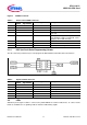
Figure 5 POWER connector
Table 4 Pinout of the POWER connector
Pin No.
Arduino
TM
Signal Name
XMC1100 Signal Name
Description
1
-
-
-
2
IOREF
VDDP
VDDP connect to 5V via R102
3
AREF
P2.4
ADC input to sense Analog reference voltage
4
3.3V
+3V3
3.3V is generated by a 3.3V regulator IC101
from +5V
5
5V
+5V
+5V is generated by the 5V regulator IC102
from VIN input. If VIN is not powered, +5V is
supply by micro-USB connector.
6
GND
GND
Ground
7
GND
GND
Ground
8
VIN
VIN
DC jack (not mounted), 7-12V
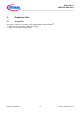
2.1.4 ICSP (In-Circuit Serial Programming) Header
The SPI connector (not mounted) is used to program the XMC1100 microcontroller via the SPI interface.
Figure 6 ICSP connector
Table 5 Signals of ICSP connector
Pin No.
Arduino
TM
Signal Name
XMC1100 Signal Name
Description
1
MISO
P1.0
Data transmit
2
+5V
VDDP
5Vdc
3
SCK
P0.7
Clock input
4
MOSI
P1.1
Data received
5
SS
P2.4
Chip select
6
GND
GND
ground
2.2 LEDs
Ardurino
TM
pinout signal ‘13-SCK’ is connected to yellow LED102 via a buffer. Furthermore, six surface mount
LEDs are available for user signaling. Table 6 shows the LEDs driving signals.