
User manual

CPU-12A-V1
XMC1200 CPU Card
Board User's Manual 9 Revision 2.0, 2013-12-18
2.2 Reset
XMC1200 does not have a reset pin, hence, user needs to unplug and replug the USB cable to achieve power-
on with master reset to the XMC1200 device.
2.3 Clock Generation
No external clock source is required. XMC1200 has two internal oscillators DCO1 and DCO2. DCO1 has a clock
output of 64MHz. DCO2 is used to generate the standby clock running at 32.768KHz which used for Real Time
Clock too. The main clock, MCLK and fast peripherial clock, PCLK, are generated from DCO1’s output.
2.4 Boot Option
After power-on with master reset, XMC1200 device will enter different boot mode depend on the BMI (Boot
Mode Index) value stored in XMC1200’s flash configuration sector 0 (CS0). The BMI value pre-programmed in
the XMC1200 CPU Card is User mode with debug enabled, hence, XMC1200 CPU Card will start to run the
application code in its embedded Flash after power on reset.
2.5 Debug Interface and virtual com port
XMC1200 CPU Card has on-board debugger which supports Serial Wire Debug (SWD) and Single Pin Debug
(SPD) as debug interface. SPD is a proprietary debugging protocol from Infineon Technologies and it requires
only 1 pin for debug communication. The debugger also provides a virtual COM port which support UART
communication via P1.3 (rx-in) and P1.2 (tx-out) of XMC1200. There is a 2x5 pins Header Debug connector
X201.
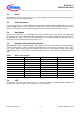
Table 1 Debug connector X201
Pin
Signal Name
XMC1200 Signal
Description
1
SWCLK
P0.15
SWD clock signal
2
SWD(SPD)
P0.14
SWD / SPD signal
3
VDDP
VDDP
+5V
4
GND
VSSP
Ground
5
GND
VSSP
Ground
6
VDDP
VDDP
+5V
7
PC_TXD
P1.3
UART data received
8
PC_RXD
P1.2
UART data transmit
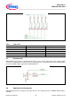
2.6 LED
The port pins P0.0, P0.2, P0.5, P0.6 and P0.7 are connected to LED101, LED102, LED103, LED104 and
LED105 respectively. The LED is turns on by output ‘Low’ at the port pin.