
Datasheet


C161K
C161O
Data Sheet 30 V2.0, 2001-01
Parameter Interpretation
The parameters listed in the following partly represent the characteristics of the C161K/
O and partly its demands on the system. To aid in interpreting the parameters right, when
evaluating them for a design, they are marked in column “Symbol”:
CC (Controller Characteristics):
The logic of the C161K/O will provide signals with the respective timing characteristics.
SR (System Requirement):
The external system must provide signals with the respective timing characteristics to
the C161K/O.
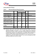
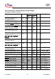
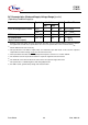
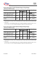
DC Characteristics (Standard Supply Voltage Range)
(Operating Conditions apply)
1)
Parameter Symbol Limit Values Unit Test Condition
min. max.
Input low voltage (TTL,
all except XTAL1)
V
IL
SR -0.5 0.2 V
DD
- 0.1
V –
Input low voltage XTAL1
V
IL2
SR -0.5 0.3 V
DD
V –
Input high voltage (TTL,
all except RSTIN
and XTAL1)
V
IH
SR 0.2 V
DD
+ 0.9
V
DD
+
0.5
V –
Input high voltage RSTIN
(when operated as input)
V
IH1
SR 0.6 V
DD
V
DD
+
0.5
V –
Input high voltage XTAL1
V
IH2
SR 0.7 V
DD
V
DD
+
0.5
V –
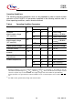
Output low voltage
(PORT0, PORT1, Port 4, ALE,
RD, WR, BHE, RSTOUT,
RSTIN
2)
)
V
OL
CC – 0.45 V I
OL
= 2.4 mA
Output low voltage
(all other outputs)
V
OL1
CC – 0.45 V I
OL
= 1.6 mA
Output high voltage
3)
(PORT0, PORT1, Port 4, ALE,
RD
, WR, BHE, RSTOUT)
V
OH
CC 2.4 – V I
OH
= -2.4 mA
0.9
V
DD
– V I
OH
= -0.5 mA
Output high voltage
3)
(all other outputs)
V
OH1
CC 2.4 – V I
OH
= -1.6 mA
0.9
V
DD
– V I
OH
= -0.5 mA
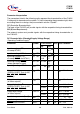
Input leakage current (Port 5)
I
OZ1
CC – ±200 nA 0 V < V
IN
< V
DD
Input leakage current (all other) I
OZ2
CC – ±500 nA 0.45 V < V
IN
< V
DD
RSTIN inactive current
4)
I
RSTH
5)
– -10 µA V
IN
= V
IH1