
Datasheet


C505/C505C/C505A/C505CA
Data Sheet 53 12.00
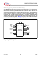
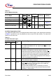
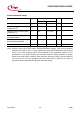
P2.0-7 18-25 I Address lines
P2.0-7 are used as multiplexed address input lines A0-A7 and
A8-A14. A8-A14 must be latched with PALE.
PSEN
26 I Program store enable
This input must be at static “0“ level during the whole
programming mode.
PROG
27 I Programming mode write strobe
This input is used in programming mode as a write strobe for
OTP memory program, and lock bit write operations During
basic programming mode selection a low level must be applied
to PROG
.
EA
/V
PP
29 – External Access / Programming voltage
This pin must be at 11.5V (V
PP
) voltage level during
programming of an OTP memory byte or lock bit. During an
OTP memory read operation this pin must be at V
IH
high level.
This pin is also used for basic programming mode selection. At
basic programming mode selection a low level must be applied
to EA
/V
PP
.
D7-0 30-37 I/O Data lines 0-7
During programming mode, data bytes are transferred via the
bidirectional port 0 data lines.
N.C. 1-3, 6, 11-13,
28, 38-44
– Not Connected
These pins should not be connected in programming mode.
*) I = Input
O= Output
Table 11
Pin Definitions and Functions in Programming Mode (cont’d)
Symbol
Pin Number
I/O
*)
Function