
Datasheet


C515C
Data Sheet 7 2003-02
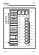
P3.0-P3.7 15-22
15
16
17
18
19
20
21
22
I/O Port 3
is an 8-bit quasi-bidirectional I/O port with internal
pullup resistors. Port 3 pins that have 1's written to
them are pulled high by the internal pullup resistors,
and in that state can be used as inputs. As inputs,
port 3 pins being externally pulled low will source
current (
I
IL
, in the DC characteristics) because of
the internal pullup resistors. Port 3 also contains the
interrupt, timer, serial port and external memory
strobe pins that are used by various options. The
output latch corresponding to a secondary function
must be programmed to a one (1) for that function to
operate. The secondary functions are assigned to
the pins of port 3, as follows:
P3.0 RXD Receiver data input (asynch.) or
data input/output (synch.) of
serial interface
P3.1 TXD Transmitter data output (asynch.)
or clock output (synch.) of serial
interface
P3.2 INT0
External interrupt 0 input / timer 0
gate control input
P3.3 INT1
External interrupt 1 input / timer 1
gate control input
P3.4 T0 Timer 0 counter input
P3.5 T1 Timer 1 counter input
P3.6 WR
WR control output; latches the
data byte from port 0 into the
external data memory
P3.7 RD
RD control output; enables the
external data memory
Table 2 Pin Definitions and Functions (cont’d)
Symbol Pin Number I/O
1)
Function
P-MQFP-80-1