
Datasheet


C515C
Data Sheet 8 2003-02
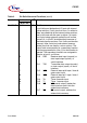
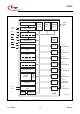
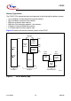
P1.0 - P1.7 31-24
31
30
29
28
27
26
25
24
I/O Port 1
is an 8-bit quasi-bidirectional I/O port with internal
pullup resistors. Port 1 pins that have 1's written to
them are pulled high by the internal pullup resistors,
and in that state can be used as inputs. As inputs,
port 1 pins being externally pulled low will source
current (
I
IL
, in the DC characteristics) because of
the internal pullup resistors. The port is used for the
low-order address byte during program verification.
Port 1 also contains the interrupt, timer, clock,
capture and compare pins that are used by various
options. The output latch corresponding to a
secondary function must be programmed to a one
(1) for that function to operate (except when used for
the compare functions). The secondary functions
are assigned to the port 1 pins as follows:
P1.0 INT3
CC0 Interrupt 3 input / compare 0
output / capture 0 input
P1.1 INT4 CC1 Interrupt 4 input / compare 1
output / capture 1 input
P1.2 INT5 CC2 Interrupt 5 input / compare 2
output / capture 2 input
P1.3 INT6 CC3 Interrupt 6 input / compare 3
output / capture 3 input
P1.4 INT2
Interrupt 2 input
P1.5 T2EX Timer 2 external reload / trigger
input
P1.6 CLKOUT System clock output
P1.7 T2 Counter 2 input
XTAL2 36 I XTAL2
Input to the inverting oscillator amplifier and input to
the internal clock generator circuits.
To drive the device from an external clock source,
XTAL2 should be driven, while XTAL1 is left
unconnected. Minimum and maximum high and low
times as well as rise/fall times specified in the AC
characteristics must be observed.
Table 2 Pin Definitions and Functions (cont’d)
Symbol Pin Number I/O
1)
Function
P-MQFP-80-1