
Datasheet


C515C
Data Sheet 10 2003-02
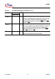
ALE 48 O The Address Latch Enable
output is used for latching the address into external
memory during normal operation. It is activated
every six oscillator periods, except during an
external data memory access. ALE can be switched
off when the program is executed internally.
EA
49 I External Access Enable
When held high, the C515C executes instructions
always from the internal ROM. When held low, the
C515C fetches all instructions from external
program memory.
Note: For the ROM protection version EA
pin is
latched during reset.
P0.0-P0.7 52-59 I/O Port 0
is an 8-bit open-drain bidirectional I/O port.
Port 0 pins that have 1's written to them float, and in
that state can be used as high-impedance inputs.
Port 0 is also the multiplexed low-order address and
data bus during accesses to external program and
data memory. In this application it uses strong
internal pullup resistors when issuing 1's.
Port 0 also outputs the code bytes during program
verification in the C515C. External pullup resistors
are required during program verification.
P5.0-P5.7 67-60 I/O Port 5
is an 8-bit quasi-bidirectional I/O port with internal
pullup resistors. Port 5 pins that have 1's written to
them are pulled high by the internal pullup resistors,
and in that state can be used as inputs. As inputs,
port 5 pins being externally pulled low will source
current (
I
IL
, in the DC characteristics) because of
the internal pullup resistors.
Port 5 can also be switched into a bidirectional
mode, in which CMOS levels are provided. In this
bidirectional mode, each port 5 pin can be
programmed individually as input or output.
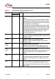
Table 2 Pin Definitions and Functions (cont’d)
Symbol Pin Number I/O
1)
Function
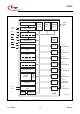
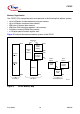
P-MQFP-80-1