
Datasheet


XC164-32
Derivatives
General Device Information
Data Sheet 15 V1.1, 2006-08
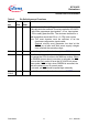
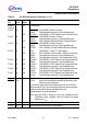
PORT1
(cont’d)
P1H.0
P1H.1
P1H.2
P1H.3
P1H.4
P1H.5
P1H.6
P1H.7
89
90
91
92
93
94
95
96
IO
I
I
I/O
I
I
I/O
I
I
I/O
I
I/O
I
I
I/O
I
I/O
I
I/O
I
I/O
I
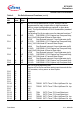
…continued…
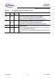
CC6POS0
CAPCOM6: Position 0 Input,
EX0IN Fast External Interrupt 0 Input (default pin),
CC23IO CAPCOM2: CC23 Capture Inp./Compare Outp.
CC6POS1
CAPCOM6: Position 1 Input,
EX1IN Fast External Interrupt 1 Input (default pin),
MRST1 SSC1 Master-Receive/Slave-Transmit In/Out.
CC6POS2
CAPCOM6: Position 2 Input,
EX2IN Fast External Interrupt 2 Input (default pin),
MTSR1 SSC1 Master-Transmit/Slave-Receive Out/Inp.
T7IN CAPCOM2: Timer T7 Count Input,
SCLK1 SSC1 Master Clock Output / Slave Clock Input,
EX3IN Fast External Interrupt 3 Input (default pin),
EX0IN Fast External Interrupt 0 Input (alternate pin A)
CC24IO CAPCOM2: CC24 Capture Inp./Compare Outp.,
EX4IN Fast External Interrupt 4 Input (default pin)
CC25IO CAPCOM2: CC25 Capture Inp./Compare Outp.,
EX5IN Fast External Interrupt 5 Input (default pin)
CC26IO CAPCOM2: CC26 Capture Inp./Compare Outp.,
EX6IN Fast External Interrupt 6 Input (default pin)
CC27IO CAPCOM2: CC27 Capture Inp./Compare Outp.,
EX7IN Fast External Interrupt 7 Input (default pin)
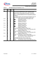
XTAL2
XTAL1
99
100
O
I
XTAL2: Output of the oscillator amplifier circuit
XTAL1: Input to the oscillator amplifier and input to the
internal clock generator
To clock the device from an external source, drive XTAL1,
while leaving XTAL2 unconnected. Minimum and maximum
high/low and rise/fall times specified in the AC.
Characteristics must be observed.
Note: Input pin XTAL1 belongs to the core voltage domain.
Therefore, input voltages must be within the range
defined for
V
DDI
.
V
AREF
28 – Reference voltage for the A/D converter.
V
AGND
29 – Reference ground for the A/D converter.
Table 2 Pin Definitions and Functions (cont’d)
Sym-
bol
Pin
Num.
Input
Outp.
Function