
Datasheet


XC164-32
Derivatives
Functional Description
Data Sheet 17 V1.1, 2006-08
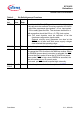
3 Functional Description
The architecture of the XC164CS combines advantages of RISC, CISC, and DSP
processors with an advanced peripheral subsystem in a very well-balanced way. In
addition, the on-chip memory blocks allow the design of compact systems-on-silicon with
maximum performance (computing, control, communication).
The on-chip memory blocks (program code-memory and SRAM, dual-port RAM, data
SRAM) and the set of generic peripherals are connected to the CPU via separate buses.
Another bus, the LXBus, connects additional on-chip resources as well as external
resources (see Figure 3).
This bus structure enhances the overall system performance by enabling the concurrent
operation of several subsystems of the XC164CS.
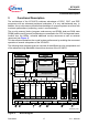
The following block diagram gives an overview of the different on-chip components and
of the advanced, high bandwidth internal bus structure of the XC164CS.
Figure 3 Block Diagram
GPT
C166SV2 - Core
DPRAM
CPU
PMU
DMU
BRGen BRGen BRGen BRGen
ASC0
USART
ASC1
USART
SSC0
SPI
SSC1
SPI
ADC
8-Bit/
10-Bit
14 Ch
CC1
T1
T0
Twin
CAN
A B
RTC WDT Interrupt & PEC
EBC
LXBus Control
External Bus
Control
DSRAM
ProgMem
Flash/ROM
256 Kbytes
PSRAM
Osc / PLL
Clock Generator
OCDS
Debug Support
XTAL
Interrupt Bus
Peripheral Data Bus
CC2
T8
T7
14
P 20 P 9 Port 5 Port 4 Port 3 PORT1 PORT0
16
16148
T6
T5
T4
T3
T2
5 6
MCB04323_X432R
LXB us
CC6
T13
T12