
Datasheet

XC164-32
Derivatives
Electrical Parameters
Data Sheet 51 V1.1, 2006-08
4 Electrical Parameters
4.1 General Parameters
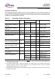
Note: Stresses above those listed under “Absolute Maximum Ratings” may cause
permanent damage to the device. This is a stress rating only and functional
operation of the device at these or any other conditions above those indicated in
the operational sections of this specification is not implied. Exposure to absolute
maximum rating conditions for extended periods may affect device reliability.
During absolute maximum rating overload conditions (
V
IN
> V
DDP
or V
IN
< V
SS
) the
voltage on
V
DDP
pins with respect to ground (V
SS
) must not exceed the values
defined by the absolute maximum ratings.
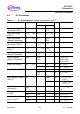
Table 9 Absolute Maximum Ratings
Parameter Symbol Limit Values Unit Notes
Min. Max.
Storage temperature
T
ST
-65 150 °C
1)
1) Moisture Sensitivity Level (MSL) 3, conforming to Jedec J-STD-020C for 260 °C for PG-TQFP-100-5, and
240 °C for P-TQFP-100-16.
Junction temperature T
J
-40 150 °C under bias
Voltage on
V
DDI
pins with
respect to ground (
V
SS
)
V
DDI
-0.5 3.25 V –
Voltage on
V
DDP
pins with
respect to ground (
V
SS
)
V
DDP
-0.5 6.2 V –
Voltage on any pin with
respect to ground (
V
SS
)
V
IN
-0.5 V
DDP
+
0.5
V
2)
2) Input pin XTAL1 belongs to the core voltage domain. Therefore, input voltages must be within the range
defined for
V
DDI
.
Input current on any pin
during overload condition
–-1010mA–
Absolute sum of all input
currents during overload
condition
– – |100| mA –