
Datasheet

XC164-32
Derivatives
Electrical Parameters
Data Sheet 56 V1.1, 2006-08
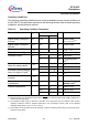
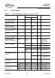
Table 12 Current Limits for Port Output Drivers
Port Output Driver
Mode
Maximum Output Current
(
I
OLmax
, -I
OHmax
)
1)
1) An output current above |I
OXnom
| may be drawn from up to three pins at the same time.
For any group of 16 neighboring port output pins the total output current in each direction (Σ
I
OL
and Σ-I
OH
) must
remain below 50 mA.
Nominal Output Current
(
I
OLnom
, -I
OHnom
)
Strong driver 10 mA 2.5 mA
Medium driver 4.0 mA 1.0 mA
Weak driver 0.5 mA 0.1 mA
Table 13 Power Consumption XC164CS (Operating Conditions apply)
Parameter Sym-
bol
Limit Values Unit Test Condition
Min. Max.
Power supply current (active)
with all peripherals active
I
DDI
– 10 +
3.0 ×
f
CPU
mA f
CPU
in [MHz]
1)2)
1) During Flash programming or erase operations the supply current is increased by max. 5 mA.
2) The supply current is a function of the operating frequency. This dependency is illustrated in Figure 11.
These parameters are tested at
V
DDImax
and maximum CPU clock frequency with all outputs disconnected and
all inputs at
V
IL
or V
IH
.
Pad supply current I
DDP
–5 mA
3)
3) The pad supply voltage pins (V
DDP
) mainly provides the current consumed by the pin output drivers. A small
amount of current is consumed even though no outputs are driven, because the drivers’ input stages are
switched and also the Flash module draws some power from the
V
DDP
supply.
Idle mode supply current
with all peripherals active
I
IDX
– 10 +
1.3 ×
f
CPU
mA f
CPU
in [MHz]
2)
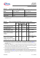
Sleep and Power down mode
supply current caused by
leakage
4)
4) The total supply current in Sleep and Power down mode is the sum of the temperature dependent leakage
current and the frequency dependent current for RTC and main oscillator (if active).
I
PDL
5)
5) This parameter is determined mainly by the transistor leakage currents. This current heavily depends on the
junction temperature (see Figure 13). The junction temperature
T
J
is the same as the ambient temperature T
A
if no current flows through the port output drivers. Otherwise, the resulting temperature difference must be
taken into account.
– 128,000
× e
-α
mA V
DDI
= V
DDImax
6)
T
J
in [°C]
α =
4670 / (273 +
T
J
)
Sleep and Power down mode
supply current caused by
leakage and the RTC running,
clocked by the main oscillator
4)
I
PDM
7)
– 0.6 +
0.02 ×
f
OSC
+
I
PDL
mA V
DDI
= V
DDImax
f
OSC
in [MHz]