
Datasheet


XC164-32
Derivatives
Electrical Parameters
Data Sheet 72 V1.1, 2006-08
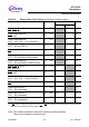
Note: The shaded parameters have been verified by characterization.
They are not subject to production test.
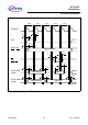
Table 22 External Bus Cycle Timing
(Operating Conditions apply)
Parameter Symbol Limit Values Unit
Min. Max.
Output valid delay for:
RD
, WR(L/H)
tc
10
CC 115ns
Output valid delay for:
BHE
, ALE
tc
11
CC -1 8 ns
Output valid delay for:
A23 … A16, A15 … A0 (on PORT1)
tc
12
CC 318ns
Output valid delay for:
A15 … A0 (on PORT0)
tc
13
CC 318ns
Output valid delay for:
CS
tc
14
CC 316ns
Output valid delay for:
D15 … D0 (write data, MUX-mode)
tc
15
CC 319ns
Output valid delay for:
D15 … D0 (write data, DEMUX-mode)
tc
16
CC 216ns
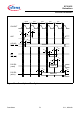
Output hold time for:
RD
, WR(L/H)
tc
20
CC -3 4ns
Output hold time for:
BHE
, ALE
tc
21
CC 0 11 ns
Output hold time for:
A23 … A16, A15 … A0 (on PORT0)
tc
23
CC 1 13 ns
Output hold time for:
CS
tc
24
CC -2 4ns
Output hold time for:
D15 … D0 (write data)
tc
25
CC 1 13 ns
Input setup time for:
D15 … D0 (read data)
tc
30
SR 29 – ns
Input hold time
D15 … D0 (read data)
1)
1) Read data are latched with the same (internal) clock edge that triggers the address change and the rising edge
of RD
. Therefore address changes before the end of RD have no impact on (demultiplexed) read cycles. Read
data can be removed after the rising edge of RD
.
tc
31
SR -5 – ns