
Datasheet


C167CR
C167SR
General Device Information
Data Sheet 20 V3.3, 2005-02
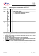
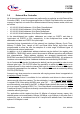
XTAL2
XTAL1
D13
C13
O
I
XTAL2: Output of the oscillator amplifier circuit.
XTAL1: Input to the oscillator amplifier and input to the
internal clock generator.
To clock the device from an external source, drive XTAL1,
while leaving XTAL2 unconnected. Minimum and maximum
high/low and rise/fall times specified in the AC
Characteristics must be observed.
RST
OUT
D12 O Internal Reset Indication Output. This pin is set to a low level
when the part is executing either a hardware-, a software- or
a watchdog timer reset. RSTOUT
remains low until the EINIT
(end of initialization) instruction is executed.
RSTIN
E11 I/O Reset Input with Schmitt-Trigger characteristics. A low level
at this pin while the oscillator is running resets the C167CR.
An internal pull-up resistor permits power-on reset using only
a capacitor connected to
V
SS
.
A spike filter suppresses input pulses < 10 ns. Input pulses
> 100 ns safely pass the filter. The minimum duration for a
safe recognition should be 100 ns + 2 CPU clock cycles.
In bidirectional reset mode (enabled by setting bit BDRSTEN
in register SYSCON) the RSTIN
line is internally pulled low
for the duration of the internal reset sequence upon any reset
(HW, SW, WDT). See note below this table.
Note: To let the reset configuration of PORT0 settle and to let
the PLL lock a reset duration of ca. 1 ms is
recommended.
Table 3 Pin Definitions and Functions P-BGA-176-2 (cont’d)
Symbol Pin
Num.
Input
Outp.
Function