
Datasheet

C167CR
C167SR
Electrical Parameters
Data Sheet 59 V3.3, 2005-02
Operating Conditions
The following operating conditions must not be exceeded in order to ensure correct
operation of the C167CR. All parameters specified in the following sections refer to these
operating conditions, unless otherwise noticed.
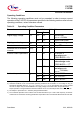
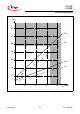
Table 10 Operating Condition Parameters
Parameter Symbol Limit Values Unit Notes
Min. Max.
Digital supply voltage
V
DD
4.5 5.5 V Active mode,
f
CPUmax
= 33 MHz
2.5
1)
1) Output voltages and output currents will be reduced when V
DD
leaves the range defined for active mode.
5.5 V Power Down mode
Digital ground voltage
V
SS
0 V Reference voltage
Overload current
I
OV
– ±5mAPer pin
2)3)
2) Overload conditions occur if the standard operating conditions are exceeded, i.e. the voltage on any pin
exceeds the specified range (i.e.
V
OV
> V
DD
+ 0.5 V or V
OV
< V
SS
- 0.5 V). The absolute sum of input overload
currents on all pins may not exceed 50 mA. The supply voltage must remain within the specified limits.
Proper operation is not guaranteed if overload conditions occur on functional pins like XTAL1, RD
, WR, etc.
3) Not subject to production test - verified by design/characterization.
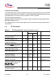
Absolute sum of overload
currents
Σ|I
OV
|– 50 mA
3)
External Load Capacitance C
L
– 50 pF Pin drivers in
fast edge mode
(PDCR.BIPEC = ‘0’)
– 30 pF Pin drivers in
reduced edge mode
(PDCR.BIPEC = ‘1’)
3)
– 100 pF Pin drivers in
fast edge mode,
f
CPUmax
= 25 MHz
4)
4) The increased capacitive load is valid for the 25 MHz-derivatives up to a CPU clock frequency of 25 MHz.
Under these circumstances the timing parameters as specified in the “C167CR Data Sheet 1999-06” are valid.
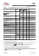
Ambient temperature T
A
070°C SAB-C167CR …
-40 85 °C SAF-C167CR …
-40 125 °C SAK-C167CR …