TLE42994V33 Low Dropout Fixed Voltage Regulator TLE42994GMV33 TLE42994EV33 Data Sheet Rev. 1.
Low Dropout Fixed Voltage Regulator 1 TLE42994GMV33 Overview Features • • • • • • • • • • • • • • • • • Output Voltage 3.
TLE42994V33 Overview Dimensioning Information on External Components The input capacitor CI is recommended for compensation of line influences. The output capacitor CQ is necessary for the stability of the control loop. Circuit Description The control amplifier compares a reference voltage to a voltage that is proportional to the output voltage and drives the base of the series transistor via a buffer. Saturation control as a function of the load current prevents any oversaturation of the power element.
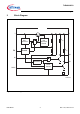
TLE42994V33 Block Diagram 2 Block Diagram TLE 4299 I Q Current and Saturation Control BandGapReference EN INH RSO RRO Inhibit Enable Control SO SI Reference RO Reset Control RADJ D GND AEB03104 Figure 1 Data Sheet Block Diagram 4 Rev. 1.
TLE42994V33 Pin Configuration 3 Pin Configuration 3.1 Pin Assignment TLE42994GMV33 (PG-DSO-14) RADJ 1 14 SI D 2 13 I GND 3 12 GND GND 4 11 GND GND 5 10 GND EN 6 9 Q RO 7 8 SO PinConfig_PG-DSO-14.vsd Figure 2 Pin Configuration (top view) 3.
TLE42994V33 Pin Configuration 3.3 Pin Assignment TLE42994EV33 (PG-SSOP-14 Exposed Pad) RADJ n.c. D GND EN n.c. RO 1 2 3 4 5 6 7 14 13 12 11 10 9 8 SI I n.c. Q n.c. n.c. SO PINCONFIG_SSOP-14.VSD Figure 3 Pin Configuration (top view) 3.4 Pin Definitions and Functions TLE42994EV33 (PG-SSOP-14 Exposed Pad) Pin Symbol Function 1 RADJ Reset Threshold Adjust connect an external voltage divider to adjust reset threshold; connect to GND for using internal threshold 2, 6 n.c.
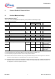
TLE42994V33 General Product Characteristics 4 General Product Characteristics 4.1 Absolute Maximum Ratings Absolute Maximum Ratings 1) -40 °C ≤ Tj ≤ 150 °C; all voltages with respect to ground, positive current flowing into pin (unless otherwise specified) Pos. Parameter Symbol Limit Values Unit Conditions Min. Max. VI, VEN, VSI -40 45 V – VQ, VRO, VSO -0.3 7 V – VD, VRADJ -0.
TLE42994V33 General Product Characteristics 4.2 Pos. Functional Range Parameter Symbol 4.2.1 Input Voltage 4.2.2 Output Capacitor’s Requirements for Stability 4.2.3 Junction Temperature Limit Values VI CQ ESR(CQ) Tj Unit Conditions Min. Max. 4.
TLE42994V33 Block Description and Electrical Characteristics 5 Block Description and Electrical Characteristics 5.1 Voltage Regulator The output voltage VQ is controlled by comparing a portion of it to an internal reference and driving a PNP pass transistor accordingly. The control loop stability depends on the output capacitor CQ, the load current, the chip temperature and the poles/zeros introduced by the integrated circuit.
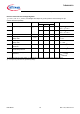
TLE42994V33 Block Description and Electrical Characteristics Electrical Characteristics Voltage Regulator VI = 13.5 V, -40 °C ≤ Tj ≤150 °C, all voltages with respect to ground, positive current flowing into pin (unless otherwise specified) Pos. Parameter Symbol 5.1.1 Output Voltage VQ Limit Values Unit Conditions Min. Typ. Max. 3.23 3.30 3.37 V 100 µA < IQ < 100 mA 5.5 V < VI < 18 V 3.20 3.30 3.40 V 100 µA < IQ < 150 mA 5.
TLE42994V33 Block Description and Electrical Characteristics 5.2 Typical Performance Characteristics Voltage Regulator Output Voltage VQ versus Junction Temperature TJ Output Current IQ versus Input Voltage VI 02_IQ_VI.VSD 400 01_VQ_TJ. VSD 3,5 350 3,4 300 V I = 13.5 V I Q = 5 mA IQ,max [mA] T j = -40 °C V Q [V] 3,3 3,2 250 T j = 25 °C T j = 150 °C 200 150 100 3,1 50 0 3 -40 10 60 110 0 160 10 20 T j [°C] 04_DVQ_DVI.
TLE42994V33 Block Description and Electrical Characteristics 1 0 -1 -2 -3 -4 -5 -6 -7 -8 Output Capacitor Series Resistor ESR(CQ) versus Output Current IQ 05_DVQ_DIQ.VSD 06_ESR_IQ.VSD 100 VI = 6 V Unstable Region 10 ESR(CQ ) [Ω ] ΔV Q [mV] Load Regulation ΔVQ,load versus Output Current Change ΔIQ T j = -40 °C T j = 25 °C T j = 150 °C 0 50 100 C Q = 22 µF T j = -40..150 °C 1 V I = 6..28 V Stable Region 0,1 0,01 150 0 50 I Q [mA] 5.
TLE42994V33 Block Description and Electrical Characteristics 5.4 Typical Performance Characteristics Current Consumption Current Consumption Iq versus Output Current IQ Current Consumption Iq versus Output Current IQ (IQ low) 08_IQ_IQ.VSD 6 09_IQ_IQ_IQLOW.VSD 1 V I = 13.5 V V I = 13.
TLE42994V33 Block Description and Electrical Characteristics 5.5 Enable Function Electrical Characteristics Voltage Regulator VI = 13.5 V, -40 °C ≤ Tj ≤150 °C, all voltages with respect to ground, positive current flowing into pin (unless otherwise specified) Pos. Parameter 5.5.1 Enable OFF Voltage Range 5.5.2 Enable ON Voltage Range 5.5.3 Enable OFF Input Current 5.5.4 Enable ON Input Current 5.6 Symbol VEN,OFF VEN,ON IEN,OFF IEN,ON Limit Values Unit Conditions Min. Typ. Max. – – 0.
TLE42994V33 Block Description and Electrical Characteristics Reset Reaction Time: The reset reaction time avoids that short undervoltage spikes trigger an unwanted reset “low” signal. The reset reaction rime trr considers the internal reaction time trr,int and the discharge time trr,d defined by the external delay capacitor CD (see typical performance graph for details).
TLE42994V33 Block Description and Electrical Characteristics I Q RRO Int. Supply Control CQ RO ID,ch RRO,ext Reset I RO VDST VRADJ,th VDD optional Supply OR RADJ,1 MicroController RADJ I RADJ GND optional ID,dch D BlockDiagram_ResetAdjust.vsd RADJ,2 GND CD Figure 5 Data Sheet Block Diagram Reset Function 16 Rev. 1.
TLE42994V33 Block Description and Electrical Characteristics VI t t < trr,total VQ VRT 1V t t rd VD V DU V DRL t VRO V RO,low t rd trr,total trd t rr,total t rd t rr,total 1V t Thermal Shutdown Figure 6 Data Sheet Input Voltage Dip Undervoltage Spike at output Overload T i mi n g Di a g ra m_ Re se t . vs Timing Diagram Reset 17 Rev. 1.
TLE42994V33 Block Description and Electrical Characteristics Electrical Characteristics Reset Function VI = 13.5 V, -40 °C ≤ Tj ≤ 150 °C, all voltages with respect to ground, positive current flowing into pin (unless otherwise specified) Pos. Parameter Symbol Limit Values Unit Conditions Min. Typ. Max. 3.00 3.10 3.20 V VQ decreasing 50 200 300 mV – Output Undervoltage Reset 5.6.1 Default Output Undervoltage Reset VRT Switching Thresholds 5.6.
TLE42994V33 Block Description and Electrical Characteristics 5.7 Typical Performance Characteristics Reset Undervoltage Reset Switching Threshold VRT versus Junction Temperature Tj Power On Reset Delay Time trd versus Junction Temperature Tj 12_TRD_TJ.VSD 70 11_VRT_TJ.
TLE42994V33 Block Description and Electrical Characteristics 5.8 Early Warning Function The additional sense comparator provides an early warning function: Any voltage (e.g. the input voltage) can be monitored, an undervoltage condition is indicated by setting the comparator’s output to low. Sense Input Voltage VSI, High VSI, Low t Sense Output High Low t AED03049 Figure 7 Sense Timing Diagram Electrical Characteristics Early Warning Function VI = 13.
TLE42994V33 Block Description and Electrical Characteristics Electrical Characteristics Early Warning Function VI = 13.5 V, -40 °C ≤ Tj ≤ 150 °C, all voltages with respect to ground, positive current flowing into pin (unless otherwise specified) Pos. Parameter Symbol Limit Values Min. Typ. Max. Unit Conditions Sense Comparator Output 5.8.5 Sense Output Low Voltage VSO,low – 0.1 0.4 V VSI < VSI,low VI > 4.4 V 5.8.6 Sense Output Internal Pull-up Resistor to VQ RSO 10 20 40 kΩ – 5.8.
TLE42994V33 Package Outlines 6 Package Outlines 1.75 MAX. C 1) 4 -0.2 B 1.27 0.64 ±0.25 0.1 2) 0.41+0.10 -0.06 6±0.2 0.2 M A B 14x 14 0.2 M C 8 1 7 1) 8.75 -0.2 8˚MAX. 0.19 +0.06 0.175 ±0.07 (1.47) 0.35 x 45˚ A Index Marking 1) Does not include plastic or metal protrusion of 0.15 max. per side 2) Lead width can be 0.61 max. in dambar area GPS01230 Figure 8 Data Sheet PG-DSO-14 22 Rev. 1.
TLE42994V33 Package Outlines 0.15 M C A-B D 14x 0.64 ±0.25 1 8 1 7 0.2 M D 8x Bottom View 3 ±0.2 A 14 6 ±0.2 D Exposed Diepad B 0.1 C A-B 2x 14 7 8 2.65 ±0.2 0.25 ±0.05 2) 0.08 C 8˚ MAX. C 0.65 0.1 C D 0.19 +0.06 1.7 MAX. Stand Off (1.45) 0 ... 0.1 0.35 x 45˚ 3.9 ±0.11) 4.9 ±0.11) Index Marking 1) Does not include plastic or metal protrusion of 0.15 max.
TLE42994V33 Revision History 7 Revision History Revision Date Changes 1.01 2010-10-14 page 10, Pos. 5.1.1: Editorial change typ. 3.0 V corrected to 3.30 V 1.0 2010-10-01 initial version data sheet Data Sheet 24 Rev. 1.
Edition 2010-10-14 Published by Infineon Technologies AG 81726 Munich, Germany © 2010 Infineon Technologies AG All Rights Reserved. Legal Disclaimer The information given in this document shall in no event be regarded as a guarantee of conditions or characteristics.