TLE6251D High Speed CAN-Transceiver with Bus Wake-up Data Sheet Rev. 1.
TLE6251D Table of Contents 1 Overview . . . . . . . . . . . . . . . . . . . . . . . . . . . . . . . . . . . . . . . . . . . . . . . . . . . . . . . . . . . . . . . . . . . . . . . 3 2 Block Diagram . . . . . . . . . . . . . . . . . . . . . . . . . . . . . . . . . . . . . . . . . . . . . . . . . . . . . . . . . . . . . . . . . . . 4 3 3.1 3.2 Pin Configuration . . . . . . . . . . . . . . . . . . . . . . . . . . . . . . . . . . . . . . . . . . . . . . . . . . . . . . . . . . . . . . . .
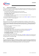
High Speed CAN-Transceiver with Bus Wake-up 1 TLE6251D Overview Features • • • • • • • • • • • • • • • • • Fully compatible with ISO 11898-2 / -5 Wide common mode range for electromagnetic immunity (EMI) Very low electromagnetic emission (EME) Excellent ESD immunity Extended supply range on VCC and VIO VIO input for voltage adaption to the microcontroller supply CAN short-circuit proof to ground, battery and VCC TxD time-out function Low CAN bus leakage current in power-down state Overtemperature prote
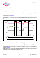
TLE6251D Block Diagram 2 Block Diagram 3 5 VCC VIO Transmitter CANH 1 7 Driver Transmitter CANL 6 TxD Timeout TempProtection 8 Mode Control STB Normal Mode Receiver * 4 Mux * Receive Unit RxD Wake-Logic & Filter Low Power Receiver VIO VCC/2 = GND 2 Figure 1 Data Sheet Block diagram 4 Rev. 1.
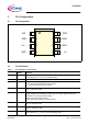
TLE6251D Pin Configuration 3 Pin Configuration 3.1 Pin Assignment TxD 1 8 STB GND 2 7 CANH VCC 3 6 CANL RxD 4 5 VIO Figure 2 Pin configuration 3.2 Pin Definitions Table 1 Pin Definitions and Functions Pin No. Symbol Function 1 TxD Transmit Data Input; Internal pull-up to VIO, “low” for “dominant” state. 2 GND Ground 3 VCC Transceiver Supply Voltage; 100 nF decoupling capacitor to GND required, VCC can be turned off in stand-by mode.
TLE6251D Functional Description 4 Functional Description CAN is a serial bus system that connects microcontrollers, sensors and actuators for real-time control applications. The use of the Controller Area Network (abbreviated CAN) within road vehicles is described by the international standard ISO 11898. According to the 7-layer OSI reference model, the physical layer of a CAN bus system specifies the data transmission from one CAN node to all other available CAN nodes within the network.
TLE6251D Functional Description The TLE6251D is a High Speed CAN transceiver, operating as an interface between the CAN controller and the physical bus medium. A HS CAN network is a two-wire, differential network, which allows data transmission rates up to 1 Mbps. The characteristics for a HS CAN network are the two signal states on the CAN bus: “dominant” and “recessive” (see Figure 3). The CANH and CANL pins are the interface to the CAN bus and both pins operate as an input and output.
TLE6251D Functional Description 4.2 Modes of Operation Two different modes of operation are available on the TLE6251D. Each mode has specific characteristics in terms of quiescent current or data transmission. The digital input pin STB is used for the mode selection. Figure 4 illustrates the different mode changes depending on the status of the STB pin. After supplying VCC and VIO to the HS CAN transceiver, the TLE6251D starts in stand-by mode.
TLE6251D Functional Description 4.3 Normal-operating Mode In the normal-operating mode, the HS CAN transceiver TLE6251D sends the serial data stream on the TxD pin to the CAN bus. The data on the CAN bus is displayed at the RxD pin simultaneously. In normal-operating mode, all functions of the TLE6251D are active: • • • • • • The transmitter is active and drives data from the TxD to the CAN bus. The receiver is active and provides the data from the CAN bus to the RxD pin.
TLE6251D Functional Description 4.6 Remote Wake-up The TLE6251D has a remote wake-up feature, also called bus wake-up feature. In stand-by mode, the low-power receiver monitors the activity on the CAN bus and in case it detects a wake-up signal, the TLE6251D indicates the wake-up signal on the RxD output pin. While entering into stand-by mode by setting the STB pin to logical “high”, the RxD output pin is set to logical “high”, regardless of the signal on the CAN bus.
TLE6251D Fail Safe Functions 5 Fail Safe Functions 5.1 Short-circuit Protection The CANH and CANL bus outputs are short-circuit proof, either against GND or a positive supply voltage. A current limiting circuit protects the transceiver against damages. If the device heats up due to a continuous short on the CANH or CANL, the internal overtemperature protection switches off the bus transmitter. 5.2 Unconnected Logical Pins All logical input pins have an internal pull-up resistor to VIO.
TLE6251D Fail Safe Functions 5.4 Undervoltage Detection The HS CAN Transceiver TLE6251D is provided with undervoltage detection on the power supply VCC and the power supply VIO. Both undervoltage detection monitors are active in normal-operating mode. In stand-by mode only the VIO undervoltage monitoring is active, the VCC undervoltage monitoring is disabled.
TLE6251D Fail Safe Functions 5.5 Overtemperature Protection The TLE6251D has an integrated overtemperature detection circuit to protect the TLE6251D against thermal overstress of the transmitter. The overtemperature protection is active in normal-operating mode and disabled in stand-by mode. In case of an overtemperature condition, the temperature sensor will disable the transmitter (see Figure 1) while the transceiver remains in normal-operating mode.
TLE6251D Fail Safe Functions First change from „recessive“ to „dominant“ t = tWU t = tWU t = tWU t = tWU CANH CANL t VDIFF = CANH - CANL VDIFF t RxD t VIO STB t normaloperating mode Figure 9 Data Sheet stand-by mode Change to stand-by mode during bus “dominant” 14 Rev. 1.
TLE6251D Fail Safe Functions 5.7 Delay Time for Mode Change During the mode change from stand-by mode to normal-operating mode or vice versa, the internal receive unit switches from the low-power receiver to the normal mode receiver and vice versa. In order to avoid any bit toggling on the RxD output pin, the RxD output is set to logical “high” during the mode change for the time tMode (see Figure 10) and is not reflecting the signal on the CAN bus.
TLE6251D General Product Characteristics 6 General Product Characteristics 6.1 Absolute Maximum Ratings Table 3 Absolute Maximum Ratings Voltages, Currents and Temperatures1) All voltages with respect to ground; positive current flowing into pin (unless otherwise specified) Pos. Parameter Symbol Limit Values Min. Max. Unit Remarks Voltages 6.1.1 Supply voltage VCC -0.3 6.0 V – 6.1.2 Logic supply voltage -0.3 6.0 V – 6.1.3 CANH DC voltage versus GND -40 40 V – 6.1.
TLE6251D General Product Characteristics 6.2 Functional Range Table 4 Operating Range Pos Parameter Symbol Limit Values Min. Max. Unit Remarks Supply Voltages 6.2.1 Transceiver supply voltage VCC 4.5 5.5 V – 6.2.2 Digital supply voltage VIO 3.0 5.5 V – Tj -40 150 °C 1) Thermal Parameters 6.2.3 Junction temperature 1) Not subject to production test, specified by design. Note: Within the functional range, the IC operates as described in the circuit description.
TLE6251D Electrical Characteristics 7 Electrical Characteristics 7.1 Functional Device Characteristics Table 6 Electrical Characteristics 4.5 V < VCC < 5.5 V; 3.0 V < VIO < 5.5 V; RL = 60 Ω; -40 °C < Tj < 150 °C; all voltages with respect to ground; positive current flowing into pin; unless otherwise specified. Pos. Parameter Symbol Limit Values Min. Typ. Max. Unit Remarks Current Consumption 7.1.
TLE6251D Electrical Characteristics Table 6 Electrical Characteristics (cont’d) 4.5 V < VCC < 5.5 V; 3.0 V < VIO < 5.5 V; RL = 60 Ω; -40 °C < Tj < 150 °C; all voltages with respect to ground; positive current flowing into pin; unless otherwise specified. Pos. Parameter Symbol Limit Values Min. Typ. Max. 0.5 × 0.7 × VIO VIO Unit Remarks Stand-by Input: STB 7.1.21 “High” level input voltage threshold VSTB,H – 7.1.22 “Low” level input voltage threshold VSTB,L 0.3 × 0.4 × VIO VIO 7.1.
TLE6251D Electrical Characteristics Table 6 Electrical Characteristics (cont’d) 4.5 V < VCC < 5.5 V; 3.0 V < VIO < 5.5 V; RL = 60 Ω; -40 °C < Tj < 150 °C; all voltages with respect to ground; positive current flowing into pin; unless otherwise specified. Pos. Parameter Symbol Limit Values Min. Typ. Max. Unit Remarks 7.1.40 CANL “dominant” output voltage VCANL 0.5 – 2.25 V VTxD = 0 V, 50 Ω < RL < 65 Ω, normal-operating mode; 7.1.41 CANH “dominant” output voltage VCANH 2.75 – 4.
TLE6251D Electrical Characteristics 7.2 Diagrams VIO 7 CANH TxD STB CL 5 100 nF 1 8 RL RxD 6 4 CRxD CANL GND VCC 3 100 nF 2 Figure 11 Simplified test circuit VTxD VIO GND VDIFF td(L),T 0,9V 0,5V t td(H),R td(L),R VRxD t td(H),T td(L),TR td(H),TR VIO 0.7 x VIO 0.3 x VIO GND t Figure 12 Data Sheet Timing diagrams for dynamic characteristics 21 Rev. 1.
TLE6251D Application Information 8 Application Information 8.1 ESD Immunity According to IEC61000-4-2 Tests for ESD immunity according to IEC61000-4-2, “GUN test” (150 pF, 330 Ω), have been performed. The results and test conditions are available in a separate test report.
TLE6251D Application Information 8.2 Application Example VBAT I Q1 22 uF TLE4476D CANH CANL EN 100 nF GND 100 nF Q2 3 VCC 22 uF 100 nF VIO 5 TLE6251D 8 STB 7 CANH 6 1 TxD Out 4 RxD CANL VCC Out In Microcontroller e.g. XC22xx Optional: Common Mode Choke GND GND 2 I Q1 22 uF TLE4476D EN GND 100 nF Q2 3 VCC 22 uF VIO TLE6251D STB 7 CANH 6 TxD RxD CANL Optional: Common Mode Choke 5 8 1 4 100 nF 100 nF VCC Out Out In Microcontroller e.g.
TLE6251D Application Information 8.3 • • Further Application Information Please contact us for information regarding the pin FMEA. For further information you may visit: http://www.infineon.com/transceiver Data Sheet 24 Rev. 1.
TLE6251D Package Outline 9 Package Outline 0.1 2) 0.41+0.1 -0.06 0.2 8 5 1 4 5 -0.2 1) M 0.19 +0.06 4 -0.2 C B 8 MAX. 1.27 1.75 MAX. 0.175 ±0.07 (1.45) 0.35 x 45˚ 1) 0.64 ±0.25 6 ±0.2 A B 8x 0.2 M C 8x A Index Marking 1) Does not include plastic or metal protrusion of 0.15 max. per side 2) Lead width can be 0.61 max.
TLE6251D Revision History 10 Revision History Revision Date Changes 1.0 2012-07-27 Data Sheet created Data Sheet 26 Rev. 1.
Edition 2012-07-27 Published by Infineon Technologies AG 81726 Munich, Germany © 2006 Infineon Technologies AG All Rights Reserved. Legal Disclaimer The information given in this document shall in no event be regarded as a guarantee of conditions or characteristics.