
Datasheet


TLE6251D
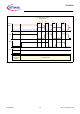
Electrical Characteristics
Data Sheet 19 Rev. 1.0, 2012-07-27
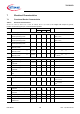
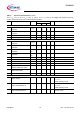
Stand-by Input: STB
7.1.21 “High” level input voltage
threshold
V
STB,H
–0.5 ×
V
IO
0.7 ×
V
IO
V stand-by mode;
7.1.22 “Low” level input voltage
threshold
V
STB,L
0.3 ×
V
IO
0.4 ×
V
IO
– V normal-operating mode;
7.1.24 STB pull-up resistance
R
STB
10 25 50 kΩ –
7.1.25 STB input hysteresis
V
HYS(STB)
–200–mV
1)
Bus Receiver
7.1.26 Differential receiver threshold
“dominant”
V
DIFF_D
– 0.75 0.9 V normal-operating mode;
7.1.27 Differential receiver threshold
“recessive”
V
DIFF_R
0.5 0.65 – V normal-operating mode;
7.1.28 Differential receiver threshold
“dominant”
V
DIFF_D_
STB
– 0.8 1.15 V stand-by mode;
7.1.29 Differential receiver threshold
“recessive”
V
DIFF_R_
STB
0.4 0.7 – V stand-by mode;
7.1.30 Common Mode Range CMR -12 – 12 V
V
CC
=5V;
7.1.31 Differential receiver hysteresis
V
diff,hys
–100–mV
1)
normal-operating mode;
7.1.32 CANH, CANL input resistance
R
i
10 20 30 kΩ “recessive” state;
7.1.33 Differential input resistance
R
diff
20 40 60 kΩ “recessive” state;
7.1.34 Input resistance deviation
between CANH and CANL
Δ
R
i
- 3–3%
1)
“recessive” state;
7.1.35 Input capacitance CANH,
CANL versus GND
C
In
– 2040pF
1)
V
TXD
= V
IO
;
7.1.36 Differential input capacitance
C
InDiff
– 1020pF
1)
V
TXD
= V
IO
;
Bus Transmitter
7.1.37 CANL/CANH “recessive”
output voltage
V
CANL/H
2.0 2.5 3.0 V no load,
V
TxD
= V
IO
,
normal-operating mode;
7.1.38 CANH, CANL “recessive”
output voltage difference
V
diff
-500 – 50 mV no load,
V
TxD
= V
IO
,
normal-operating mode;
7.1.39 CANH, CANL “recessive”
output voltage difference
V
diff
-0.1 – 0.1 V no load,
stand-by mode;
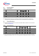
Table 6 Electrical Characteristics (cont’d)
4.5 V <
V
CC
< 5.5 V; 3.0 V < V
IO
< 5.5 V; R
L
=60Ω; -40 °C<T
j
<150°C; all voltages with respect to ground;
positive current flowing into pin; unless otherwise specified.
Pos. Parameter Symbol Limit Values Unit Remarks
Min. Typ. Max.