.4 Dimension The dimension of SB52 is 55 mm x 45 mm x 3.5 mm. Detail dimension please see Fig1-2. Figure 1-2 SB52 SOM Dimension 1.5 Electrical Specifications Symbol VSYS VSYS Parameter Input Voltage Input Current Minimum Maximum 3.4 4.35 1.5 Unit V A Table 1-1: Input Power Absolute Maximum Ratings Symbol VIO28_PMU VIO18_PMU Parameter VDDIO_2V8 VDDIO_1V8 Minimum 2.66 1.71 Table 1-2: Output Power www.innocomm.com6 Maximum 2.94 1.
Symbol T Parameter Operating Temp. Minimum Maximum 0 60* Unit °C Table 1-3 Operating Temperature Note * : Test with heat sink 1.6 General Application Notes Consider the following recommendations when designing application boards: • • • • • Use a GND plane underneath the SB52. Do not use vias in high-speed interface lines such as USB and Ethernet. Rout high-speed interface lines differentially and leave several mm gap to other signal lines when possible.
2 Main Hardware Components SB52 SOM has two 75-pin M.2 E-key golden fingers to connect with another carrier board. It integrates MTK the i500, LPDDR4 Memory, eMMC, Power Manage IC (PMIC), and WiFi/Bluetooth on the module. Figure 2-1 – Top side of SB52 SOM Figure 2-2 – Bottom side of SB52 SOM www.innocomm.
2.1 CPU MTK i500 processor integrates a multi-core ARM® Cortex-A73, ARM® Cortex-A53 MPCore equipped with the NEON engine offers processing power necessary to support the latest OpenOs along with its demanding applications such as web browsing, email, GPS navigation, and games. The features of i500 processors include the following: • • • • Quad-core ARM Cortex-A73 MPCore operating at 2GHz Quad-core ARM Cortex-A53 MPCore operating at 2GHz NEON multimedia processing engine ARM TrustZone security 2.
MTK MT6358 power management IC is used for SB52 SOM. MT6358 is a programmable power management IC that integrates 9 buck converters and 33 LDOs to provide all power rails required by SoC and peripherals. MT6358 adopts the SPI interface and two SRCLKEN control pins to control buck converters, LDOs, and various drivers; it provides enhanced safety control and protocol for handshaking with i500.
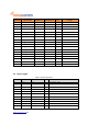
3 SB52 SOM Interfaces and Connectors SB52 use two M.2 E-key golden finger to connect with the carrier board. The tables below detail the pin assignment and functionality of these connectors. 3.1 J401 Connector Table 3-1 J401 Connector J401 Pin # 1 2 3 4 5 6 7 8 9 10 11 12 13 14 15 16 17 18 19 20 21 22 23 Signal Name SYSRSTB VBAT PWRKEY_SW VBAT VCAMA2_PMU VBAT GND VBAT GND GND AUXIN4 VBUS GPIO9 VRTC28 GPIO17 GPIO10 UCTS1 GPIO22 SDA2 GPIO23 SCL2 GPIO24 AU_MICBIAS0 www.innocomm.
J401 Pin# 32 33 34 35 36 37 38 39 40 41 42 43 44 45 46 47 48 49 50 51 52 53 54 55 56 57 58 59 60 61 62 63 64 65 66 Signal Name SPI_CSB AU_VIN2_N SPI_CLK AU_VIN0_P SPI_MI AU_VIN0_N SPI_MO AU_REFN URTS1 AU_HPR GPIO19 AU_HPL GPIO150 GND I2S1_LRCK AU_MICBIAS1 I2S1_BCK AU_VIN1_P I2S1_DO AU_VIN1_N KPROW0 ACCDET URXD1 HP_EINT UTXD1 GND KPCOL0 USB_DM KPROW1 USB_DP KPCOL1 GND SDA1 SDA3 SCL1 www.innocomm.
J401 Pin# 67 68 69 70 71 72 73 74 75 Signal Name SCL3 GPIO0 GND GPIO20 SDA0 GPIO42 SCL0 GPIO8 VIO18_PMU I500 Pin # AF22 AB5 MT6358 Pin # Y24 AC5 AF26 AB6 AD4 F3 I/O I/O I/O GND I/O I/O I/O I/O I/O PO Voltage 1.8 1.8 I/O AGND PO GND I/O I/O I/O I/O I/O I I/O I/O I/O I/O I/O I/O I/O DSI I/O Voltage 1.8 1.8 1.8 1.8 1.8 1.8 3.
J402 Pin# 19 20 21 22 23 32 33 34 35 36 37 38 Signal Name DSI0_D2P DSI0_D3N DSI0_D1N DSI0_D3P DSI0_D1P DSI0_CKP DSI0_D0N DSI0_CKN DSI0_D0P CAM_CLK0 RDN3 RDN2 I500 Pin # V25 T24 T26 T25 U26 U25 R27 U24 T27 AA4 T1 P3 MT6358 Pin # I/O DSI DSI DSI DSI DSI DSI DSI DSI DSI I/O CSI CSI 39 RDP3 T2 CSI 40 41 RDP2 RDN1 P4 R4 CSI CSI 42 RCP P5 CSI 43 44 45 46 47 48 49 50 RDP1 RCN RDN0 GND RDP0 RDN3_A GND RDP3_A R3 N5 R1 CSI CSI CSI GND CSI CSI GND CSI 51 VCAMA_PMU 52 RDN2_A 53 VCAMD_PMU 54 5
J402 Pin# 58 59 60 61 62 63 Signal Name GND RCP_A GPIO3 RCN_A VMCH_PMU GND 64 GPIO177 65 66 67 68 69 70 71 72 73 74 75 CAM_CLK1 I2S1_DI GND I2S1_MCK RDN1_A GPIO6 RDP1_A GPIO5 RDN0_A GPIO4 RDP0_A I500 Pin # MT6358 Pin # N1 AG1 N2 R10 AC2 AD27 AD20 N4 AE2 N3 AF2 M4 AC3 M3 I/O GND CSI I/O CSI PO GND Voltage 1.8 2.9/3/3.3 I/O 1.8 I/O I/O GND I/O CSI I/O CSI I/O CSI I/O CSI 1.8 1.8 1.8 1.8 1.8 1.8 3.
3.4 I2Cs Parameter Specification SB52 SOM I2C is an open-drain interface, the specification is shown in Table 3-5. Table 3-4 I2C parameter specificaition Parameters Description Min Typ Max Unit VIH Input logic high voltage 0.65*VDD VDD+0.3 V VIL Input logic low voltage -0.3 0.35*VDD V VOL DC output low voltage 0.2*VDD V * VDD is 1.
Table 3-6 UART Signal Pins Connector# PIN# PIN name I/O Description J402 5 UART_RXD0 I UART0_RXD J402 7 UART_TXD0 O UART0_TXD J401 54 URXD1 I UART1_RXD J401 56 UTXD1 O UART1_TXD J401 17 UCTS1 I UART1_CTS J401 40 URTS1 O UART1_RTS 3.
3.7 CSI Interface SB52 SOM provides 2 MIPI CSI high-speed camera serial interface with 4 data lane ( for main and sub ) and throughput up to 2.8G bps for 1 data lane.
3.8 Audio SB52 SOM provides a Master I2S input/output interface from I500, 2 PDM interface for DMIC and 1 earphone interface from MT6358.
3.9 USB SB52 SOM provides high speed USB functionality conforms to the USB2.0. The OTG controller conforms to OTG2.0 specification. Table 3-12 USB Signal Pins Connector# PIN# PIN name I/O Description J401 61 USB_DP I/0 USB DP J401 59 USB_DM I/0 USB DM J402 11 IDDIG I USB ID J401 12 VBUS P USB VBUS 3.10 GPIO All the IOs from i500 can be configured to GPIO purposes. For more detail pin-mux table please see the reference documents [1]. 4 Reference Documents 1. 2. 3.
5 How to Process SB52 SB52 is base on Android 10 OS , to access SB52, please install display share tools in PC If you have no ADB driver, You can find ADB driver from web side or download form android link There are many APPs you can use, you can download tools from web side: For example: 1. Google Vyser Vysor lets you view and control your Android on your computer. Easy peasy. Please find Vysor App under link: http://www.vysor.io/download/ 2.
Home The Home screen is your starting point for using the applications on your SB52. There are many programs on applications , Enjoy the SB52 !! www.innocomm.
Setting Wireless connection: 1.Quick setting: Swipe down to show quick setup options 2.1 Normal setting: To have WLAN and BT connection www.innocomm.
1. Make device discoverable: Under “Settings”, choose “Connected devices”. Tap “Bluetooth” to turn on it and tap “Search for devices”. The Bluetooth indicator then appears in the status bar. 2. Scan for devices: After scanning, there will be a list of the IDs of all available Bluetooth devices in range. If the device you want to pair with isn’t in the list, ensure that the other device is turned on and set to be discoverable. 3.
1. 2. 3. Make device discoverable: Under “Settings”, choose “Network and internet”. Tap “Wi-iFi” to turn on it and Searching Access Point devices. Scan for devices: After scanning, there will be a list of the APs SSID of all available APs devices in range. If the device you want to connect with isn’t in the list, ensure that the other device is turned on and set to be discoverable. Connect to the WLAN APs: Tap the name of an available Bluetooth device to pair with.
Federal Communication Commission Interference Statement 15.19 This device complies with Part 15 of the FCC Rules. Operation is subject to the following two conditions: (1) this device may not cause harmful interference, and (2) this device must accept any interference received, including interference that may cause undesired operation. 15.105 This equipment has been tested and found to comply with the limits for a Class B digital device, pursuant to part 15 of the FCC Rules.
which integrates this module. 20cm minimum distance has to be able to be maintained between the antenna and the users for the host this module is integrated into. Under such configuration, the FCC radiation exposure limits set forth for an population/uncontrolled environment can be satisfied. Any changes or modifications not expressly approved by the manufacturer could void the user's authority to operate this equipment.
Antennas Brand name Model name Antenna type Antenna gain Antenna connector BJTEK TH96-120mmipex & Holder Monopole 3.14(dBi) ipex Label and Compliance Information Product manufacturers need to provide a physical or e-label stating “Contains FCC ID: YAISB52” with finished product Information on Test Modes and Additional Testing Requirements Test tool: Android debug bridge shall be used to set the module to transmit continuously. www.innocomm.