
Data Sheet


www.
inno
tec
hsm
art
.
c
om
4
-
7
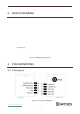
3.2 Pin Description
Table 1: Pin Definitions
Name
No.
Type
Function
VDD_3V3
1
P
Power supply (3.0-3.6V)
GND
2
P
Ground
PWM1
3
I/O
PWM output1, GPIO4
PWM2/SDA
4
I/O
PWM output2, GPIO5
I2C data line
PWM3/SCL
5
I/O
PWM Output3, GPIO6
I2C clock line
PWM4
6
I/O
PWM Output4, GPIO7
PWM5
7
I/O
PWM Output5, GPIO10
TXD
8
I/O
UART TX, connect to host RX, GPIO18
RXD
9
I/O
UART RX, connect to host TX, GPIO19
ADC1
10
I/O
ADC input, GPIO3
4. ELECTRICAL CHARACTERISTICS
4.1 Absolute Maximum Ratings
Stresses beyond the absolute maximum ratings listed in the table below may cause permanent damage to the
device. These are stress ratings only, and do not refer to the functional operation of the device that the
recommended operating conditions.
Table 2: Absolute Maximum Ratings
Symbol
Parameter
Min
Max
Unit
VDD_3V3
Power supply voltage
-0.3
3.6
V
T
store
Storage temperature
-40
105
˚C
4.2 Recommended Operating Conditions
Table 3: Recommended Operating Conditions
Symbol
Parameter
Min
Type
Max
Unit
VDD_3V3
Power supply voltage
3.0
3.3
3.6
V
I
VDD
Current delivered by external power
supply
0.5
--
--
A
T
A
Operating temperature
-40
--
105
˚C
Humidity
Humidity condition
--
--
85
%RH
4.3 DC Characteristics (3.3V, 25˚C)
Table 4: DC Characteristics (3.3V, 25˚C)