Features: Standard ATA/IDE Bus Interface - 512 Bytes / Sector ATA command set compatible Selectable Master/Slave Setting Capacities - 8GB up to 64GB (SLC or MLC) Data Transfer mode - Support Data Transfer up to PIO mode 6 Support Data Transfer up to Multiword DMA mode 2 Support Data Transfer up to Ultra DMA mode 5 Performance - - Integral Z Series (MLC) Sustain Read Speed up to 43MB/s Sustain Write Speed up to 36MB/s Integral E Series (SLC) (Pls call for availability) Sustain Read S
TABLE OF CONTENTS 1.0 BLOCK DIAGRAM ..................................................................................................................... 4 2.0 SPECIFICATION ........................................................................................................................ 4 2.1 PIN ASSIGNMENTS ................................................................................................................ 4 2.2 PIN DESCRIPTION..........................................................
1.0 Block Diagram 2.0 Specification 2.
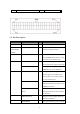
43* GND 44* NC * Note: Pin 41~44 only for 44pin AFM 2.2 Pin Description Pin No. Signal I/O* Description 01 -RESET I Hardware reset signal from the host 17,15,13,11,09,07, DD0~DD15(Device Data) I/O 16-bit bi-direction Data Bus. DD(7:0) are 05,03,04,06,08,10, used for 8-bit register transfers. 12,14,16,18 21 DMARQ(DMA Request) O For DMA data transfers. Device will assert DMARQ when the device is ready to transfer data to or from the host.
acknowledge) 31 INTRQ(Interrupt) to DMARQ to initiate DMA transfer. O When this device is selected, this signal is the active high Interrupt Request to the host Pin No. Signal I/O Description 32 IOIS16 O During PIO transfer mode0,1or 2, this pin indicates to the host the 16-bit data port has been addressed and the device is prepared to send or receive a 16-bit data word. When transferring in DMA mode, the host must use a 16-bit DMA channel and this signal will not be asserted.
“Pin41~44” Only for 44pin AFM 2.3 Jumper Setting Follow diagram define AFM Master/Slave Jumper (J2) settings 2.3.1 44pin (H/V) Jumper Settings Master Slave Cable Select 44pin Horizontal 44pin Vertical 2.3.
2.3.
3.0 Electrical Characteristics 3.1 Absolute Maximum Rating Item Symbol Parameter MIN MAX Unit 1 VDD-VSS DC Power Supply -0.3 +5.5 V 2 VIN Input Voltage Vss-0.3 VDD+0.3 V 3 Ta Operating Temperature 0 +70 0C 4 Tst Storage Temperature -25 +85 0C Parameter Symbol MIN TYP MAX Unit VDD Voltage VDD 3.0 3.3 3.6 V 4.5 5.0 5.5 V 3.2 DC Characteristics of 5.
3.3 AC Characteristics 3.3.
PIO timing parameters t0 Cycle time t1 Address valid to (min) DIOR-/DIOW- setup (min) t2 DIOR-/DIOW- (min) t2i DIOR-/DIOW- recovery time Mode 0 Mode 1 Mode2 Mode 3 Mode 4 Note ns ns ns ns ns 600 383 240 180 120 70 50 30 30 25 165 125 100 80 70 1 -- -- -- 70 25 1 1,4 (min) t3 DIOW- data setup (min) 60 45 30 30 20 t4 DIOW- data hold (min) 30 20 15 10 10 t5 DIOR- data setup (min) 50 35 20 20 20 t6 DIOR- data hold (min) 5 5 5 5 5 t6z
negated at the time tA after the activation of DIOR- or DIOW-, then tRD shall be met and t5 is not applicable. 4. Mode may be selected at the highest mode for the device if CS(1:0) and DA(2:0) do not change between read or write cycle or selects at the highest mode supported by the slowest device if CS(1:0) and DA(2:0) do change between read or write cycles. 3.3.
(Sustaining a Multiword DMA data burst) (Device terminating a Multiword DMA data burst) 13
(Host terminating a Multiword DMA data burst) Multiword DMA timing parameters Mode 0 Mode 1 Mode2 ns ns ns Note t0 Cycle time (min) 480 150 120 See note tD DIOR-/DIOW- asserted pulse width (min) 215 80 70 See note tE DIOR- data access (max) 150 60 50 tF DIOR- data hold 5 5 5 tG DIOR-/DIOW- data setup 100 30 20 tH DIOW- data hold (min) 20 15 10 tI DMACK to DIOR-/DIOW- setup (min) 0 0 0 tJ DIOR-/DIOW- to DMACK hold (min) 20 5 5 tKR DIOR- negated pulse w
as appropriate) is the minimum DIOR-/DIOW- negation time. A host shall lengthen tD and/or tK to ensure that t0 is equal to the value reported in the devices IDENTIFY DEVICE data. 3.3.
Ultra DMA data burst timing descriptions 16
(Initialing an Ultra DMA data-in burst) (Sustained Ultra DMA data-in burst) 17
(Device terminating an Ultra DMA data-in burst) (Host terminating an Ultra DMA data-in burst) 18
(Initialing an Ultra DMA data-out data burst) (Sustained Ultra DMA data-out burst) 19
(Host terminating an Ultra DMA data-out burst) (Device terminating an Ultra DMA data-out burst) 20
3.4 Power Management System Power Consumption: (Ta = 0 to 700C) Symbol Parameter Conditions MIN TYP MAX Unit Iccr Read current 5V - 100 - mA Iccw Write current 5V - 105 - mA Ipd Power down current 5V - 0.2 0.4 mA Iccr Read current 3.3V - 150 - mA Iccw Write current 3.3V - 160 - mA Ipd Power down current 3.3V - 0.3 - mA 4.0 Software Interface 4.
4 CFA Write Multiple w/o Erase CDh -- Y Y Y Y Y Y 5 CFA Write Sector w/o Erase 38h -- Y Y Y Y Y Y 6 Check Power Mode E5h -- -- -- -- Y -- -- 7 Execute Device Diagnostic 90h -- -- -- -- Y -- -- 8 Identify Device ECh -- -- -- -- Y -- -- 9 Idle E3h -- Y -- -- Y -- -- 10 Idle Immediate E1h -- -- -- -- Y -- -- 11 Initialize Device Parameters 91h -- Y -- -- Y Y -- 12 NOP 00h -- -- -- -- Y -- -- 13 Read Buffer E4h -- --
Non-removable device 1 xxxxh 2 Default number of cylinders 2 0000h 2 Reserved 3 xxxxh 2 Default number of heads 4 7E00h 2 Retired 5 0200h 2 Retired 6 xxxxh 2 Default number of sectors per track 7-8 xxxxh 4 Number of sectors per device 9 0000h 2 Retired 10-19 xxxxh 20 Serial Number in ASCII 20 0002h 2 Retired 21 0002h 2 Retired 22 0004h 2 Number of ECC Bytes passed on Read/Write Long Commands 23-26 Aaaah 8 Firmware revision in ASCII 27-46 xxxxh 40 Model n
120nsec Manufacturer’s recommended Multiword DMA 66 0078h 2 transfer cycle time 120nsec Minimum PIO transfer cycle time without flow 67 0078h 2 control 120nsec Minimum PIO transfer cycle time with IORDY flow 68 0078h 2 control 120nsec 69-79 0000h 26 Reserved 80 0030h Major version number 81 0000h Reserved 82 7009h 2 Supports Security Mode feature set 83 5004h 2 Reserved 84 4000h 85 7009h Feature Setting 86 1004h Feature Setting 87 4000h Feature Setting 88 203Fh Ultra
5.0 Physical Dimension 5.1 44pin Horizontal Note: 1. Unit: mm 2. General Tolerance: ± 0.
5.2 44pin Vertical Note: 1. Unit: mm 2. General Tolerance: ± 0.
5.3 40pin Vertical Note: 1. Unit: mm 2. General Tolerance: ± 0.
5.
5.5 40pin Horizontal (Connector at bottom) Note: 1. Unit: mm 2. General Tolerance: ± 0.