
User's Manual

18 21555 Non-Transparent PCI-to-PCI Bridge User Manual
Introduction
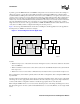
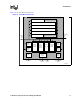
2.2 Architectural Overview
This section describes the buffers, registers, and control logic of the 21555:
2.2.1 Data Buffers
Data buffers include the buffers along with the associated data path control logic. Delayed transaction buffers
contain the compare functionality for completing delayed transactions. The blocks also contain the watchdog timers
associated with the buffers. The data buffers are as follows:
• Four-entry downstream delayed transaction buffer.
• Four-entry upstream delayed transaction buffer.
• 256-byte downstream posted write buffer.
• 256-byte upstream posted write buffer.
• 256-byte downstream read data buffer.
• 256-byte upstream read data buffer.
• Two downstream I20 delayed transaction entries.
2.2.2 Registers
The following register blocks also contain address decode and translation logic, I20 message unit, and interrupt
control logic:
• Primary interface header Type 0 configuration registers.
• Secondary interface header Type 0 configuration registers.
• Device-specific configuration registers.
• Memory and I/O mapped control and status registers.
2.2.3 Control Logic
• The 21555 has the following control logic:
• Primary PCI target control logic.
• Primary PCI master control logic.
• Secondary PCI target control logic.
• Secondary PCI master control logic.
• ROM interface control logic for both serial and parallel ROM connections (interfaces between the ROM
registers and ROM signals).
• Secondary PCI bus arbiter interface to secondary bus device request and grant lines, as well as the 21555
secondary master control logic.
• JTAG control logic.