
Datasheet


Datasheet 69
Register Description
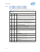
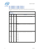
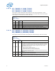
2.10.11 MC_CHANNEL_0_RANK_TIMING_B
MC_CHANNEL_1_RANK_TIMING_B
MC_CHANNEL_2_RANK_TIMING_B
This register contains parameters that specify the rank timing used. All parameters are
in DCLK.
Device: 4, 5, 6
Function: 0
Offset: 84h
Access as a Dword
Bit Type
Reset
Value
Description
20:16 RW 0
B2B_CAS_DELAY.
Controls the delay between CAS commands in DCLKS. The minimum spacing is
4 DCLKS. Values below 3 have no effect. A value of 0 disables the logic. Setting
the value between 3-31 also spaces the read data by 0-29 DCLKS. The value
entered is one less than the spacing required, i.e. a spacing of 5 DCLKS
between CAS commands (or 1 DCLK on the read data) requires a setting of 4.
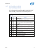
15:13 RW 0
tddWrTWr.
Minimum delay between writes to different DIMMs.
000 = 2
001 = 3
010 = 4
011 = 5
100 = 6
101 = 7
110 = 8
111 = 9
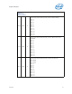
12:10 RW 0
tdrWrTWr.
Minimum delay between writes to different ranks on the same DIMM.
000 = 2
001 = 3
010 = 4
011 = 5
100 = 6
101 = 7
110 = 8
111 = 9
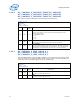
9RW0
tsrWrTWr.
Minimum delay between writes to the same rank.
0 = 4
1 = 6
8:6 RW 0
tRRD.
Specifies the minimum time between activate commands to the same rank.
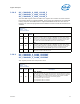
5:0 RW 0
tFAW.
Four Activate Window. Specifies the time window in which four activates are
allowed the same rank.