Intel® 41110 Serial to Parallel PCI Bridge Design Guide March 2006 Order Number: 310335-001
INFORMATION IN THIS DOCUMENT IS PROVIDED IN CONNECTION WITH INTEL® PRODUCTS. NO LICENSE, EXPRESS OR IMPLIED, BY ESTOPPEL OR OTHERWISE, TO ANY INTELLECTUAL PROPERTY RIGHTS IS GRANTED BY THIS DOCUMENT.
Contents Contents 1 About This Document ................................................................................................................... 7 1.1 2 Introduction.................................................................................................................................... 9 2.1 2.2 2.3 2.4 2.5 2.6 2.7 3 Interrupts.............................................................................................................................29 PCI Arbitration ...........
Contents 10.2 11 41110 Reference and Compensation Pins ......................................................................... 48 41110 Customer Reference Boards ........................................................................................... 51 11.1 11.2 11.3 11.4 12 Board Stack-up ................................................................................................................... 51 Material ..................................................................................
Contents 10 11 12 13 14 15 16 17 18 19 20 21 22 23 24 25 Embedded PCI-X 133 MHz Routing Recommendations ............................................................36 Embedded PCI-X 100 MHz Routing Recommendations ............................................................37 PCI-X 66 MHz Embedded Routing Recommendations ..............................................................38 PCI 66 MHz Embedded Table ................................................................................................
Contents Revision History vi Date Revision March 2006 001 Description Initial release.
1 About This Document This document provides layout information and guidelines for designing platform or add-in board applications with the Intel® 41110 Serial to Parallel PCI Bridge (also called the 41110 Bridge). It is recommended that this document be used as a guideline. Intel recommends employing best-known design practices with board level simulation, signal integrity testing and validation for a robust design.
About This Document Table 1. Terminology and Definitions (Sheet 2 of 2) Term Definition Printed circuit board. Layer 1: copper Prepreg Layer 2: GND Core PCB Layer 3: VCC15 Prepreg Layer 4: copper Example manufacturing process consists of the following steps: • Consists of alternating layers of core and prepreg stacked • The finished PCB is heated and cured.
Introduction 2 The Intel® 41110 Serial to Parallel PCI Bridge integrates a PCI Express-to-PCI bridge. The bridge follows the PCI-to-PCI Bridge programming model. The PCI Express port is compliant to the PCI Express Specification, Revision 1.0. The PCI bus interface is fully compliant to the PCI Local Bus Specification, Revision 2.3. 2.1 PCI Express Interface Features • • • • • • • 2.2 PCI Express Specification, Revision 1.0b compliant.
Introduction • Up to two downstream delayed (memory read, I/O read/write and configuration read/write) transaction. • Tunable inbound read prefetch algorithm for PCI MRM/MRL commands • Local initialization via SMBus • Secondary side initialization via Type 0 configuration cycles. 2.3 Power Management • Support for PCI Express Active State Power Management (ASPM) L0s link state • Support for PCI PM 1.
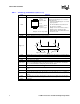
Introduction Figure 1. Microcontroller Block Diagram Serial to Parallel PCI Bridge 2.4.2 Microcontroller Connections to the 41110 Figure 2 shows the SMB interface from the 41110 to the microcontroller.
Introduction Figure 2. 41110 Microcontroller Connections Serial to Parallel PCI Bridge 2.5 JTAG • Compliant with IEEE Standard Test Access Port and Boundary Scan Architecture 1149.1a 2.6 Related Documents • • • • • • • 12 . PCI Express Specification, Revision 1.0, from www.pci-sig.com. PCI Express Design Guide, Revision 0.5 PCI Local Bus Specification, Revision 2.3, from www.pci-sig.com. PCI-X Addendum to the PCI Local Bus Specification, Revision 1.0a, from www.pci-sig.com.
Introduction Figure 3. 41110 Block Diagram Serial to Parallel PCI Bridge 2.7 Intel® 41110 Serial to Parallel PCI Bridge Applications This section provides a block diagram for a typical the 41110 application. This application shows a PCI-E adapter card with two Dual 2Gb Fibre Channel controllers. Each of the PCI-X bus segments is connected to the Dual 2Gb Fibre Channel chip running at 133MHz. The two Dual FC chips provides the four 2Gb/s outputs.
Introduction Figure 4.
3 Package Information 3.1 Package Specification The 41110 Bridge is in a 567-ball FCBGA package, 31mm X 31mm in size, with a 1.27mm ball pitch (see Figure 5 and Figure 6). Figure 5. 41110 Bridge Package Dimensions (Top View) Handling Exclusion Area 0. 491in. 0. 291in. 0. 547in. 0. 247in. Die Keepout Area 17. 00 mm 21. 00 mm 31. 00 mm 0. 200in. 17. 00 mm 21. 00 mm 31.
Package Information Figure 6. 41110 Bridge Package Dimensions (Side View) Substrate 2.445±0.102 mm 2.010±0.099 mm 0.84±0.05 mm Decoup Cap Die 0.7 mm Max 0.20 See Note 4. 0.20 -C- Seating Plane 0.435±0.025 mm See Note 3 See Note 1 Notes: 1. Primary datum -C- and seating plan are defined by the spherical crowns of the solder balls (shown before motherboard attach). 2. All dimensions and tolerances conform to ANSI Y14.5M-1994 3. BGA has a pre-SMT height of 0.5 mm and post-SMT height of 0.41-0.
4 Power Plane Layout This chapter provides details on the decoupling and voltage planes needed to bias the 41110 package. 4.1 41110 Decoupling Guidelines Table 2 lists the decoupling guidelines for the 41110. Figure 7 and Figure 8 provide the decoupling capacitors around the 41110 ball grid pins. Figure 7.
Power Plane Layout Figure 8. Decoupling Placement for PCI/PCI-X 1.5V and 3.3V Voltage Planes Capacitor Legend 0603-0.
Power Plane Layout Table 2. 4.2 41110 Decoupling Guidelines Voltage Plane Voltage 41110 Bridge Pins C (uF) Package ESR (mΩ) ESL (nH) # of Caps Location PCI/PCI-X Voltage 3.3V VCC33 0.1 0603 50300 1.03.0 5 Beneath 41110 Bridge BGA PCI/PCI-X Voltage 3.3V VCC33 1.0 0603 50300 1.03.0 2 As close as design rules will allow to 41110 Bridge BGA PCI/PCI-X Voltage 3.3V VCC33 10 1206 50300 1.03.0 3 As close as design rules will allow to 41110 Bridge BGA Core Voltage 1.
Power Plane Layout Note: Linear voltage regulators are recommended when using 1.5 Volt power supplies. Figure 9.
41110 Reset and Power Timing Considerations 5 This chapter describes the 41110 reset timing considerations. 5.1 A_RST# and PERST# Timing Requirements The PCI-X Specification requires that there is a 100ms delay from valid power (PERST#) to reset deassertion (A_RST#). 41110 will keep A_RST# asserted for a minimum of 320ms after PERST# is deasserted. 5.2 VCC15 and VCC33 Voltage Requirements The following steps are the power sequencing requirements that must be followed with the 41110: 1.
41110 Reset and Power Timing Considerations This page intentionally left blank.
General Routing Guidelines 6 This chapter provides some basic routing guidelines for layout and design of a printed circuit board using the 41110. The high-speed clocking required when designing with the 41110 requires special attention to signal integrity. In fact, it is highly recommended that the board design be simulated to determine optimum layout for signal integrity. The information in this chapter provides guidelines to aid the designer with board layout.
General Routing Guidelines Figure 10. Crosstalk Effects on Trace Distance and Height Reduce Crosstalk: P - Maximize P H aggressor victim - Minimize H Reference Plane A9259-01 • Avoid slots in the ground plane. Slots increases mutual inductance thus increasing crosstalk. • Make sure that ground plane surrounding connector pin fields are not completely cleared out.
General Routing Guidelines 6.4 Power Distribution and Decoupling Have ample decoupling to ground, for the power planes, to minimize the effects of the switching currents. Three types of decoupling are: the bulk, the high-frequency ceramic, and the inter-plane capacitors. • Bulk capacitance consist of electrolytic or tantalum capacitors. These capacitors supply large reservoirs of charge, but they are useful only at lower frequencies due to lead inductance effects.
General Routing Guidelines Note: 6.5.1 Using stripline transmission lines may give better results than microstrip. This is due to the difficulty of precisely controlling the dielectric constant of the solder mask, and the difficulty in limiting the plated thickness of microstrip conductors, which can substantially increase cross-talk. Differential Impedance The PCI Express standard defines a 100 Ω differential impedance.
7 Board Layout Guidelines This chapter provides details on adapter card stackup suggestions. It is highly recommended that signal integrity simulations be run to verify each 41110 PCB layout especially if it deviates from the recommendations listed in these design guidelines. 7.1 Adapter Card Topology The 41110 will be implemented on PCI-E adapter cards with an eight layer stackup PCB. The specified impedance range for all adapter card implementations will be 60Ω +/-15%.
Board Layout Guidelines Note: Each interface will set the trace spacing based on its signal integrity of differential impedance requirements. For the purposes of the building the transmission line models, it is assumed the artwork is very accurate and therefore a constant. All the variability in the trace spacing is the result of the tolerances of the trace width. Figure 14.
PCI-X Layout Guidelines 8 This chapter describes several factors to be considered with a 41110 PCI/PCI-X design. These include the PCI IDSEL, PCI RCOMP, PCI Interrupts and PCI arbitration. 8.1 Interrupts PCI Express provides interrupt messages that emulate the legacy wired mechanism. This allows IO devices to signal PCI-style interrupts using a pair of ASSERT and DEASSERT messages This message pairing preserves the level-sensitive semantics of the PCI interrupts on PCI Express.
PCI-X Layout Guidelines Note: 8.1.1 PCI Express Assert_INTx/Deassert_INTx messages are not inhibited by the BME bit. Interrupt Routing for Devices Behind a Bridge Given the legacy interrupt sharing scheme shown in Table 5, to get the best legacy interrupt performance (by reducing interrupt sharing), adapter boards have to select the appropriate A_INTX# (where X is A, B, C or D) input pin to use on the PCI bus segment.
PCI-X Layout Guidelines • Bus parking on last PCI agent or the bridge. By default, the arbiter parks the bus on the bridge and drives the A/D, C/BE# and PAR lines to a known value while the bus is idle. 8.2.1 PCI Resistor Compensation Figure 15 provides the recommended resistor compensation pin termination for the PCI A bus. Figure 15. PCI RCOMP RCOMP 100 Ω – 1% B2718 -01 8.
PCI-X Layout Guidelines Table 6. PCI-X Signals A PCI Bus Segment: Timing Critical Signals Reset Signals Non Timing Critical Signals Table 7. Note: 8.3.
PCI-X Layout Guidelines distributed to each PCI device. The 41110 provides seven buffered clocks on the PCI bus to connect to multiple PCI-X devices. The Figure 16 shows the use of four PCI “A” clock outputs and length matching requirements. . The recommended clock buffer layout are specified as follows: • Match each of the used the 41110 output clock lengths A_CLK[6:0] to within 0.1”to help keep the timing within the 0.5 ns maximum budget.
PCI-X Layout Guidelines Table 8.
PCI-X Layout Guidelines 8.5 PCI-X Topology Layout Guidelines The PCI-X Addendum to the PCI Local Bus Specification, Revision 1.0a compliant, recommends the following guidelines for the number of loads for your PCI-X designs. Any deviation from these maximum values requires close attention to layout with regard to loading and trace lengths. Table 9. 8.
PCI-X Layout Guidelines 8.6.1 Embedded PCI-X 133 MHz This section lists the routing recommendations for PCI-X 133 MHz without a slot. Figure 17 shows the block diagram of this topology and Table 10 describes the routing recommendations. Figure 17. Embedded PCI-X 133 MHz Topology TL_EM1 EM1 TL_EM2 TL1 EM2 B2719 -01 Table 10.
PCI-X Layout Guidelines 8.6.2 Embedded PCI-X 100 MHz This section lists the embedded routing recommendations for PCI-X 100 MHz. Figure 18 shows the block diagram of this topology and Table 11 describes the routing recommendations. Figure 18. Embedded PCI-X 100 MHz Topology EM1 TL_EM1 TL1 TL_EM3 EM3 TL_EM2 EM2 B2720 -01 Table 11.
PCI-X Layout Guidelines 8.6.3 PCI-X 66 MHz Embedded Topology Figure 19 and Table 12 provide routing details for a topology with an embedded PCI-X 66 MHz application. PCI-X 66 MHz Embedded Routing Topology TL_EM7 TL_EM8 TL4 TL_EM6 TL3 TL_EM4 TL2 EM7 TL_EM2 TL1 EM5 TL_EM3 EM3 TL_EM1 EM1 TL_EM5 Figure 19. EM2 EM4 EM6 EM8 B2721 -01 Table 12.
PCI-X Layout Guidelines 8.6.4 PCI 66 MHz Embedded Topology Figure 20 and Table 13 provide routing details for a topology with an embedded PCI 66 MHz design. Figure 20. PCI 66 MHz Embedded Topology TL_EM4 TL2 TL_EM2 TL1 TL_EM3 EM3 TL_EM1 EM1 EM2 EM4 B2722 -01 Table 13.
PCI-X Layout Guidelines 8.6.5 PCI 33 MHz Embedded Mode Topology Figure 21 and Table 14 provide routing details for a topology with an embedded PCI 33 MHz design. Figure 21. PCI 33 MHz Embedded Mode Routing Topology TL_EM9 TL_EM10 TL5 TL_EM8 TL4 TL_EM6 TL3 TL_EM4 TL2 EM9 TL_EM7 TL_EM5 EM7 TL_EM2 TL1 EM5 TL_EM3 EM3 TL_EM1 EM1 EM2 EM4 EM6 EM8 EM10 B2723 -01 Table 14.
PCI Express Layout 9 This section provides an overview of the PCI-Express stackup recommended based on Intel presimulation results. For additional information, refer to the Intel® 41110 Serial to Parallel PCI Bridge Developer’s Manual or the PCI Express Specification, Revision 1.0 from the www.pcisig.com website. 9.1 General recommendations PCI Express is a serial differential low-voltage point-to-point interconnect. The PCI Express was designed to support 20 inches between components with standard FR4.
PCI Express Layout 9.2 PCI-Express Layout Guidelines The layout guidelines for PCI-Express were developed for an adapter card topologies. The models and assumptions used in development of these guidelines were as follows: • • • • • • • • • • • Add-In Card Stackup: 60 Ω single-ended impedance Target Differential Impedance: 100 Ω +/- 20%. Driver Model: 41110 PCI-E IBIS Receiver Model: 41110 PCI-E IBIS. Specification model did not meet specifications Driver Package Model: Preliminary 41110 model.
PCI Express Layout Table 15. Adapter Card Routing Recommendations (Sheet 2 of 2) Receive Trace Length (Card edge finger to 41110 receiver pin 1.0” min - 6.0” max Length Matching Requirements: Total allowable intra-pair length mis-match must not exceed 25 mils. Each routing segment should be matched as close as possible. Total skew across all lanes must be less than 20 ns.
PCI Express Layout This page intentionally left blank.
Circuit Implementations 10 Circuit Implementations This chapter describes 41110 circuit implementations. 10.1 41110 Analog Voltage Filters The 41110 requires several external analog voltage filter circuits to be placed on the system board, three for the PCI interface, one for the PCI Express interface, and one for the bandgap voltage.
Circuit Implementations 10.1.1 PCI Analog Voltage Filters The following filter circuit is recommended for the PCI interface. Three separate, identical versions of this circuit should be placed on the system board, one for each VCCAPCI[2:0] pin on the 41110. Figure 22. PCI Analog Voltage Filter Circuit Serial to Parallel PCI Bridge Note: Three of these PCI filter circuits must be placed on the system board, one for each of the VCCAPCI[2:0] pins on the 41110. • • • • • • 10.1.
Circuit Implementations Figure 23. PCI Express Analog Voltage Filter Circuit Serial to Parallel PCI Bridge Additional Notes: • • • • • • 10.1.3 Place C as close as possible to package pin. R must be placed between VCC15 and L. Route VCCAPE and VSSAPE as differential traces. VCCAPE and VSSAPE traces must be ground referenced (No VCC15 references). Max total board trace length = 1.2”. Min trace space to other nets = 30 mils.
Circuit Implementations Figure 24. Bandgap Analog Voltage Filter Circuit Serial to Parallel PCI Bridge Additional Notes: • • • • • • • 10.2 Place C as close as possible to package pin. R must be placed between the 2.5V supply and L. Route VCCBGPE and VSSBGPE as differential traces. VCCBGPE and VSSBGPE traces must be ground referenced (No 2.5V references). VSSBGPE should be grounded at the capacitor. Max total board trace length = 1.2”. Min trace space to other nets = 30 mils.
Circuit Implementations Figure 25. Reference and Compensation Circuit Implementations Serial to Parallel PCI Bridge 10.2.1 SM Bus The SMBus interface does not have configuration registers. The SMBus address is set by the states of pins SMBUS[5] and SMBUS [3:1] when PERST# is asserted as described in Table 17. Table 17. SMBUs Address Configuration Bit Value 7 1 6 1 5 SMBUS[5] 4 0 3 SMBUS[3] 2 SMBUS[2] 1 SMBUS[1] Refer to Section 2.
Circuit Implementations This page intentionally left blank.
41110 Customer Reference Boards 11 This chapter describes the 41110 Customer Reference Board (CRB). 11.1 Board Stack-up The proposed layout of the PCB is eight layers with the following stackup: • • • • • • • • Signal #1 (Top/Component Side) Ground Plane: GND Signal #2 Power Plane Power Plane Signal #3 Ground Plane Signal #4 (Bottom) The permittivity constant Er = 4.5 Table 18. CRB Board Stackup (Sheet 1 of 2) Layer Type Thickness (mils) Copper Weight 1 Signal 2.00 1/2 + plating Prepreg 4.
41110 Customer Reference Boards Table 18. CRB Board Stackup (Sheet 2 of 2) Layer Type Thickness (mils) Copper Weight 1 Signal 2.00 1/2 + plating Prepreg 4.50 2 Plane: GND 1.20 Core 4.80 Signal 1.20 3 8 Est. Total Thickness 11.2 Prepreg 4.50 Signal 2.00 1 1 1/2 + plating 62 +/- 7 Material The following materials are used with the 41110 CRB: • FR-4, 0.062 in. +/- .007, 1.0 oz Copper Power/GND. • Full length PCI Raw Card (3.3V Universal) 6.2” high x 7.
41110 Customer Reference Boards 11.4 Board Outline Figure 26 provides the mechanical outline of the 41110 CRB. Figure 26.
41110 Customer Reference Boards This page intentionally left blank.
12 Design Guide Checklist This checklist highlights design considerations that should be reviewed prior to manufacturing an adapter card that implements the 41110 product. The items contained within this checklist attempt to address important connections to these devices and any critical supporting circuitry. This is not a complete list and does not guarantee that a design will function properly. Table 19.
Design Guide Checklist Table 20. PCI/PCI-X Interface Signals (Sheet 1 of 2) Signals Recommendations Reason/Impact A_AD[63:32] A_CBE[7:4]# A_DEVSEL# A_FRAME# A_IRDY# A_TRDY# 41110 has internal pullup resistors on these signals. A_STOP# A_PERR# No external pullup resistors required on system board. A_SERR# A_REQ[5:0]# X_AD[31:0] and X_CBE#[3:0] signals do not require pullups according to the PCI Specification.
Design Guide Checklist Table 20. PCI/PCI-X Interface Signals (Sheet 2 of 2) Signals Recommendations Reason/Impact Controls frequency of the PCI segment when running in conventional PCI mode (33 MHz or 66 MHz): 0 = 33 MHz PCI A_M66EN 1 = 66 MHz PCI • Pull-up using a 8.2KΩ resistor when the PCI bus is to operate at 66 MHz and not already pulled up by system board. This signal is grounded for 33 MHz operation. Sampled on the rising edge of PERST#.
Design Guide Checklist Table 21. Miscellaneous Signals Signals Recommendations Reason/Impact Input pin to configure 41110 to retry configuration accesses on it's PCI Express interface. CFGRETRY • To retry configuration accesses to the 41110, pull high to 3.3V through a 2K Ω resistor. • A_TEST1, A_TEST2, A_PME#, A_STRAP[3], A_STRAP[4], A_STRAP[5], CMODE To allow configuration accesses to the 41110, ground this pin through a 2K Ω resistor. These signals REQUIRE an external pull-up, 8.2KΩ to 3.3V.
Design Guide Checklist Table 23.
Design Guide Checklist Table 24. Power and Ground Signals Signal Recommendations Reason/Impact 100Ω ±1% (1/4 W) pulldown resistor to ground. Analog compensation pin for PCI. 0.75V nominal. RCOMP The trace impedance of this signal should be < 0.1Ω. Connect to 1.5V power supply. Note: Linear voltage regulators are recommended when using 1.5 Volt power supplies. Decoupling: VCC15 5 0.1uF caps beneath package (backside of board) 1.5V ±5% core voltage. 2 1.
Table 25. JTAG Signals Signal Recommendations Reason/Impact TCK If not used for JTAG, leave as No Connect Internal pull-up TDI If not used for JTAG, leave as No Connect Internal pull-up TDO If not used for JTAG, leave as No Connect Internal pull-up TMS If not used for JTAG, leave as No Connect Internal pull-up TRST# Connect to ground via a 1KΩ pulldown resistor. If TAP interface is not used this should be tied to ground.
Design Guide Checklist This page intentionally left blank.