
Computer Hardware User Manual


Intel® 41110 Serial to Parallel PCI Bridge Design Guide 23
General Routing Guidelines 6
This chapter provides some basic routing guidelines for layout and design of a printed circuit board
using the 41110. The high-speed clocking required when designing with the 41110 requires special
attention to signal integrity. In fact, it is highly recommended that the board design be simulated to
determine optimum layout for signal integrity. The information in this chapter provides guidelines
to aid the designer with board layout. Several factors influence the signal integrity of a 41110
design. These factors include:
• power distribution
• minimizing crosstalk
• decoupling
• layout considerations when routing the PCI Express bus and PCI-X bus interfaces
6.1 General Routing Guidelines
This section details general routing guidelines for designing with the 41110. The order in which
signals are routed varies from designer to designer. Some designers prefer to route all clock signals
first, while others prefer to route all high-speed bus signals first. Either order can be used, provided
the guidelines listed here are followed.
6.2 Crosstalk
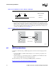
Crosstalk is caused by capacitive and inductive coupling between signals. Crosstalk is composed of
both backward and forward crosstalk components. Backward crosstalk creates an induced signal on
victim network that propagates in the opposite direction of the aggressor signal. Forward crosstalk
creates a signal that propagates in the same direction as the aggressor signal.
Circuit board analysis software is used to analyze your board layout for crosstalk problems.
Examples of 2D analysis tools include Parasitic Parameters from ANSOFT
*
and XFS from Quad
Design
*
. Crosstalk problems occur when circuit etch lines run in parallel. When board analysis
software is not available, the layout should be designed to maintain at least the minimum
recommended spacing for bus interfaces.
• A general guideline to use is, that space distance between adjacent signals be a least 3.3 times
the distance from signal trace to the nearest return plane. The coupled noise between adjacent
traces decreases by the square of the distance between the adjacent traces.
• It is also recommended to specify the height of the above reference plane when laying out
traces and provide this parameter to the PCB manufacturer. By moving traces closer to the
nearest reference plane, the coupled noise decreases by the square of the distance to the
reference plane.