
Computer Hardware User Manual


48 Intel® 41110 Serial to Parallel PCI Bridge Design Guide
Circuit Implementations
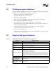
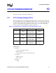
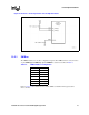
Figure 24. Bandgap Analog Voltage Filter Circuit
Additional Notes:
• Place C as close as possible to package pin.
• R must be placed between the 2.5V supply and L.
• Route VCCBGPE and VSSBGPE as differential traces.
• VCCBGPE and VSSBGPE traces must be ground referenced (No 2.5V references).
• VSSBGPE should be grounded at the capacitor.
• Max total board trace length = 1.2”.
• Min trace space to other nets = 30 mils.
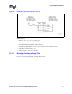
10.2 41110 Reference and Compensation Pins
There are three compensation pins on 41110.
PE_RCOMP[1:0] are two separate pins that provide voltage compensation for the PCI Express
interface on the 41110. The nominal compensation voltage is 0.5V. An external 24.9
Ω ±1% pullup
resistor should be used to connect to VCC15. A single pullup resistor can be used to for both of
these signals.
RCOMP is an analog PCI interface compensation pin, providing 0.75V to the 41110. A 100
Ω ±1%
pulldown resistor should be used to connect the RCOMP pin to ground.
These implementations are shown in Figure 25.
Serial to
Parallel PCI
Bridge