
Computer Hardware User Manual

Intel® 460GX Chipset Software Developer’s Manual 11-37
LPC/FWH Interface Configuration
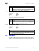
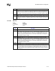
11.2.8.2 Global Status Register
Address Offset: 1Ch-1Dh
Attributes: Read/Write
Default Value: 0000h
Size: 16 bits
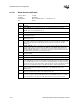
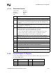
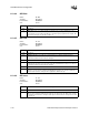
11.2.9 General Purpose I/O Registers
For the following GPIO Registers, bits 28:16 refer to the Muxed GPIO signals, and bits 8:0 refer to
the dedicated GPIO signal.
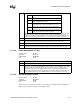
Bit Description
15:11 Reserved.
10 ECC_STS: This bit is set when ECCINT# asserted for more than 1 PCI clock with the ECC SERR#
bit in configuration space set, or for one or more clocks if the ECC SERR# bit is not set. The
setting of this bit will cause an SMI if the ECC_EN bit in the Global Control and Enable register
(offset 1A-1Bh) is set. This bit is only set by hardware and can only be cleared by writing a 1 to this
bit position.
9 BIOSWEN_STS: This bit is set when the BIOSWEN bit in configuration register 4Eh of Function 0
is set. The setting of this bit will cause an SMI. This bit is only set by hardware and can only be
reset by writing a one to this bit position.
8 EXTSMI_STS: This bit is set when a GPIO is programmed as an input, is routed to generate an
SMI#, and its register bit is set. Additionally if the EXTSMI_EN bit is set, the setting of the
EXTSMI_STS bit will cause the following, depending on the current state:
If in the S0/C0, S0/C1 or S0/C2 states: An SMI event will be generated.
If in an S1 state, then a Wake event will be generated, and SMI# will also be generated.
If in an S3-S5 state, a Wake event will be generated, but no SMI# will be generated.
This bit is only set by hardware and can only be reset by writing a one.
7 SWSMI_TMR_STS: This bit will be set to 1 by the hardware when the Software SMI# Timer
expires. This bit will remain 1 until software writes a 1 to this bit. The default of this bit is 0.
6 1MIN_STS: This hardware will set this bit to 1 when the 1-minute timer expires. This will also
cause an SMI#. This bit will remain a 1 until the software writes a 1 to this bit. The default of this bit
is 0.
5 GP_REG_STS: This bit is an OR of the bits in the ACPI General Purpose Register (offset 0Ch).
4 PM1_REG_STS: This bit is an OR of the Power Management 1 Status Register (offset 00h) bits.
3 APM_STS: SMI# was generated by a write access to the APM control register. An SMI is
generated when the APMC_EN bit is set. This bit is cleared by writing a 1.
2 Reserved.
1 LEGACY_USB_STS: This bit is an OR of the SMI status bits in the USB Legacy Keyboard
Register ANDed with the enable bits.
0 BIOS_STS: SMI# was generated due to ACPI software requesting attention (writing a 1 to the
GBL_RLS bit with the BIOS_EN bit set). This bit is set by hardware and cleared by software writing
a 1.
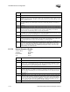
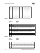
Bit GPIO Bit GPIO
28 GPIO[22] 8 GPIO[8]
27 GPIO[21] 7 GPIO[7]
26 GPIO[20] 6 GPIO[6]