
Computer Hardware User Manual


Memory Subsystem
5-2 Intel® 460GX Chipset Software Developer’s Manual
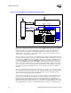
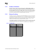
Each card is organized as 2 stacks of up to 4 rows each. A stack consists of 1 to 4 rows of DRAM
which share a common data bus. A row consists of the 4 DIMM sockets which have a common
address/control bus. A row is the minimum atomic unit that can be accessed. Each stack has a
separate data path from the MDC to the DRAMs. Data may be transferring on both stacks
simultaneously. For instance, on the same card, stack L could be doing a read while stack R is
doing a write, or both could be doing a read.
Each row represents a set of memory devices simultaneously selected by a RAS signal and having
a common address bus. Each row generates 288 bits (256 data, 32 ECC) of data. Each row uses 4 of
the x72 (168 pin) DIMMs. There may be multiple banks per row. For instance, SDRAMs have 2, 4
or 8 banks internal to the chip. Or the DIMM may be organized such that there are 2 groups of
memory on the DIMM itself (double-sided DIMMs), with 2 chips dotted together on the data pin.
Since a row provides 256 bits (32 bytes) of data, the 64 byte line transfers of the processor will
access a row twice to read or write the entire line. Data is interleaved by the MDCs to exchange 72
bits of data per transfer with the SDCs at the rate of one cache line every 30ns (2.13 GB/s) per
interface.
There is a separate address and control bus for each memory port, with 1 card on each port. These
are independent and may be driving addresses at the same time. While one bus is driving a read, the
other could be driving a write from the write queue. This allows greater bandwidth and allows
writes to be done without interfering with read traffic.
A system may be built with only one card, and provide only half the possible bandwidth, or have
the memory on the motherboard itself. If there are 2 memory cards, then one is placed on each
interface. Average memory latency is a function of how many interleaves are available and
bandwidth. The present structure interleaves across cards first, then across stacks, and then rows.
With 2 cards, each having 2 stacks of memory, Line 0 would be on cardB/stackR, Line 1 would be
on cardA/stackR, Line 2 would be on card B/stackL, and Line 3 would be on cardA/stackL. See
Figure 5-1. Maximum Memory Configuration Using Two Cards
x 72
x 72
x 72 x 72
x 72
x 72
x 72 x 72
MAC
288 bits
288 bits
MDC MDC
MDC MDC
Stack A
Stack B
MAC
SAC
MAa[24:0]
MDa[71:0]
SDC
PB[71:0]
controls
memory card A
processor address bus
to PCI via expander bridge
MDb[71:0]
processor data bus
MAb[24:0]
x 72
x 72
x 72 x 72
x 72
x 72
x 72 x 72
MAC
288 bits
288 bits
MDC
MDC MDC
Stack L
Stack R
MDC
row 1 of 4
row 4 of 4
row 1 of 4
row 4 of 4