
Intel Xeon Processor and Intel E7500/E7501Chipset Compatible Platform Design Guide


Platform Power Delivery Guidelines
174 Intel
®
Xeon™ Processor and Intel
®
E7500/E7501 Chipset Compatible Platform Design Guide
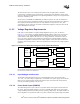
11.1.1 12 V
System designs may require user access to energized areas of the system. In these cases the power
supply may be required to meet regulatory 240 VA limits for any power rail. Since the +12 V rail
combined power exceeds 240 VA it must be divided into separate channels to meet this
requirement. Each separate rail needs to be limited to less than 20 A for each +12V rail. +12V1 is
dedicated for providing power to the input of the processor voltage regulator. The +12V2 rail is
used to power the rest of the board +12 V power needs and peripherals devices, such as the 1.2 V,
1.8 V, and 2.5 V regulators.
11.1.2 Processor Core Voltage
The processor core voltage power plane is used to power the processors. The processor core
voltage operates between 1.30 V and 1.50 V. A VRM 9.1 compatible design is required for all Intel
Xeon processor based platforms. The Voltage Regulator solution can be either a VRM 9.1 or a
VRD design. The voltage regulator solution can be either a Voltage Regulator Module (VRM) 9.1
or Voltage Regulator Down (VRD)-based design that meets the Voltage Regulator Module (VRM)
9.1 DC-DC Converter Design Guidelines or Dual Intel
®
Xeon™ Processor Voltage Regulator
Down (VRD) Design Guidelines respectively. The processor core voltage plane also provides
power to the MCH system bus signal I/O buffers and termination.
11.1.3 2.5 V
The 2.5 V power plane is used to provide power to the DDR DRAM core, the MCH DDR IO ring,
and reference voltage to the 1.25 V switching regulator. The 2.5 V power plane is created using a
switching regulator, which should be able to support up to 26 A of current. This switching regulator
receives its input directly from the 5 V power rail of the power supply. The DDR DRAM core
requires at most 20.0 A of current. This value is a worst-case current, and is based on DRAM
vendor specific specification for maximum current. Power levels will vary. In some cases, current
requirements may be less than half of this maximum value, but a maximum current level of 20.0 A
should be used to allow interoperability among DRAM devices. The current dedicated for VDD in
the MCH is 6.8 A. This regulator is required in all designs.
11.1.4 1.25 V
A voltage regulator derived off 2.5 V produces two 1.25 V rails. One is for the MCH reference
voltage (VREF); the other is for DDR termination voltage (VTERM). The switching regulator
divides the 2.5 V power rail by 2 to drive 1.25 V reference voltage. This provides some common-
mode noise rejection between the DDR termination and I/O voltages. The entire power plane
requires about 12 A of maximum current, and can be achieved by using either one or two
regulators (one for both channels or one for each channel).
11.1.5 1.8 V
There are two 1.8 V power planes on the reference design. One is created using a switching
regulator sourcing from the 5 V power rail on the power supply delivering a bulk of the platform
1.8 V current. This powers the 1.2 V regulator and the hub interface I/O rings of the P64H2s,
totaling approximately 8.42 A. A secondary linear voltage regulator is used to supply the 1.8 V rail
for the ICH3-S to ensure that the ICH3-S 1.8 V rail is never more than 2 V less than the 3.3 V rail.
The hub interface on each P64H2 device consumes about 2.66 A. The hub interface on the ICH3-S
device consumes about 550 mA of current.