
ITP700 Debug Port Design Guide

R
ITP700 Debug Port Design Guide 15
DBA# and DBR# are output signals from the ITP. The ITP provides an open drain FET closure to
GND as the drive of DBA# and DBR#. The target system should provide the pull-up for both of
these signals. The pull-up can be to any voltage up to five volts that is consistent with the input
specifications of the component used to receive these signals on the target system. DBR# is the
ITP debug port reset signal that should always be routed to the system reset controller. DBA# is
the ITP debug port scan active signal used to indicate that the ITP is currently driving the scan
chain. DBA# is an optional signal of the debug port.
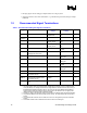
1.3.2 JTAG Signal Layout Guidelines
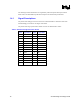
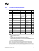
Table 3. JTAG Signal Layout Guidelines
Debug Port Signal Layout Guideline
TCK This is a critical JTAG clock signal, sourced by the debug port, which requires
thorough timing and signal integrity analysis/simulation. The termination
resistor to GND on TCK must be located within 200 ps of the debug port in
order to minimize IR losses that would degrade signal voltage levels at the
loads. The length of TCK should not exceed 2 ns in electrical length. Note that
TCK returns a feedback copy of TCK to FBO at the debug port. The length of
the trace between the processor TCK pin and the debug port must be equal to
the electrical length of BPM[5:0] and RESET# from the processor to the debug
port. Load capacitance at the processor must be no more than 35 pF. It is
strongly recommended that this signal be simulated for signal integrity
purposes. Non-monotonicity on the rising or falling edge of TCK will render the
ITP inoperative. See the Execution Signal Layout Guidelines section of this
chapter for additional information.
TMS Critical JTAG mode select signal, sourced by the debug port, which requires
moderate timing and signal integrity analysis / simulation. The termination
resistor to VTAP on TMS should be located within 200 ps of the debug port in
order to minimize resistive losses that would degrade signal voltage levels at
the loads. TMS is driven on the falling edge of TCK at the ITP and recovered
on the following rising edge of TCK at the processor.
TDI, TDO JTAG scan data signals. These signals require minor timing and signal
integrity analysis / simulation. The terminations should be located within 300 ps
to each load. TDI is driven on the falling edge of TCK at the ITP and recovered
on the following rising edge of TCK at the processor.
TRST# Non-critical JTAG reset signal routed to all scan chain devices. TRST#
requires a pull-down resistor to ensure the signal is held in the asserted (low)
state if the debug port is not driving the signals. Layout of this signal needs to
be such that noise will not be coupled to the signal and cause a false reset of
the scan chain.
For a uniprocessor scan-chain that does not include a other scan chain components: The TDI pin
of the ITP is connected to the TDI pin of the processor with the pull-up located within 200 ps of
the processor. The TDO pin of the processor is routed back to the TDO pin of the debug port with
the pull-up located within 200 ps of the debug port.