
ITP700 Debug Port Design Guide


R
60 ITP700 Debug Port Design Guide
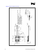
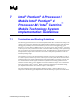
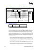
Figure 17 – BPM[5:0]# Connectivity for Intel
®
Pentium
®
4 Processor, Intel
®
Pentium
®
4
Processor-M, and Systems Based on Intel
®
Centrino
™
Mobile Technology
D
ebug Port
Connector
BPM[0]#
Signal
BPM[1]#
Signal
BPM[2]#
Signal
BPM[3]#
Signal
Rt
Rt Rt
Rt
Rt
Rt
Vcc
BPM#
012345
Chipset
Rt
Rt Rt
Rt
Rt
Rt
Vcc
BPM#
012345
uProcessor
L
BP
M
Table 34. BPM[5:0]# Figure Definitions
Parameter Min Nominal Max Notes
L
BPM
1 ns 1
NOTES:
1. BPM[5:0]# must be length matched to within 50 ps of themselves and RESET#.
Exception 1. Additional pins on the Pentium 4 socket support interposer based debug ports. The
system bus and TAP port typically cannot provide a stable BCLK(p/n) pair and a method to
provide a request for reset to the system reset controller (DBR#). The Pentium 4 socket provides
three pins to ease the implementation of an interposer based debug port. One pin is a path for
DBR# from the interposer debug port to be routed to the system reset controller. The other pair is
a path for a dedicated BCLK(p/n) pair to be routed with the interposer based ITP as the only load.
All three pins are isolated from the processor die. It is strongly recommended that a debug port be
implemented on the motherboard if it is possible. Ideally a motherboard design will allow for the
use of a motherboard based debug port or an interposer based debug port by following the routing
requirements for all signals.
In order to support an interposer debug port, The Pentium 4 processor DBR# pin must be
connected to the system reset controller with a pull-up to a voltage consistent with the input
interface of the reset controller. Systems designed to support both motherboard based as well
as interposer based debug ports must connect the motherboard debug port DBR# pin with the
processor DBR# pin and the reset controller.
In order to support an interposer debug port, the ITP_BCLK(p/n) pins on the processor socket
must have a dedicated clock pair from the system clock source. This clock pair must be routed
with the same routing rules as a processor clock. Systems designed to support both
motherboard based as well as interposer based debug ports must have two dedicated clock