
ITP700 Debug Port Design Guide


R
68 ITP700 Debug Port Design Guide
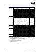
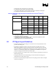
Signal DPA Type Min Typ Max Unit Note
LVDPA 0 0.1*VTAP V 1
I
OH
ITP700DPA -5 mA
LVDPA -8 mA
I
OL
ITP700DPA 5 mA
TRST#
(cont.)
LVDPA 8 mA
V
IH
ITP700DPA 0.90 1.7 V
LVDPA 0.5*VTAP
+0.150
V
V
IL
ITP700DPA 0 0.55 V
LVDPA 0.5*VTAP -
0.150
V
I
IH
ITP700DPA -150 µA
LVDPA -100 µA
I
IL
ITP700DPA 300 µA
TDO
LVDPA 100 µA
NOTES:
1. At maximum current specified.
2. As measured into a 27 Ω 1% resistor to GND.
3. AC Impedance of the driver.
4. As measured into a 39 Ω 1% resistor to 1.10 V.
5. Open Drain Driver on the LVDPA
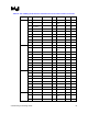
Table 37. ITP Execution Signal DC Electrical Characteristics for the Intel
®
Itanium
®
2
Processor
Signal Min Max Unit Note
I
OL
120 mA 1
R
OL
18 Ω 2
BPM5DR#
C
IN
4 pF 3
V
IH
PWR + 0.15 3.00 V 4, 5
V
IL
PWR - 0.15 V 4, 5
I
IH
-150 µA
I
IL
300 µA
BPM[5:0]#,
RESET#
C
IN
3 pF 3
NOTES:
1. Maximum sink current of the ITP.
2. Series resistance to GND when output is low.
3. Includes capacitive effects of mated connector.
4. Over valid range of VIH of PWR.
5. For Itanium 2 processor-based scan chains, PWR of the ITP debug port must be pulled up to 1.2 V
through a 1.8 kΩ 1% tolerance resistor