
ITP700 Debug Port Design Guide


R
ITP700 Debug Port Design Guide 71
8.2.1 System Signal Layout Guidelines
The following are additions to the ITP700 Debug Port Design Guide’s System Signal Layout
Guidelines.
BCLK(p/n) In addition to the generic MP guidelines in this guide, the BCLK for I/O domain
debug ports should be routed with the same length as the clocks to the Intel
®
Itanium
®
2 processor chipset components within that domain.
BCLK routing rules for miscellaneous debug ports depend on the use of the
debug port. If synchronous recovery of information routed to BPM signals is
required, the timing relationship of that interface will determine BCLK routing
rules.
FBO The routing rules for FBO for I/O domain debug ports and miscellaneous debug
ports are determined by solving the timing analysis for TDO recovery from the
last load of the scan chain.
DBR# It is possible that the DBR# pin can be used to reset only a portion of the target
system (e.g. only one processor node), but some method must be provided for
the ITP to reset the entire target system through assertions of one or more
DBR# pins.
8.2.2 JTAG Signal Layout Guidelines
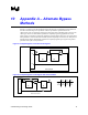
In order for the standard I/O Domain debug port and the standard miscellaneous debug port to
actively communicate with the PXB, SCSI, or similar components, the scan chain must be
(voltage) translated from the ITP drive levels to 3.3V (i.e., PXB drive level). This translation is
not a trivial design task. There are several signal integrity and scan chain continuity issues that
must be understood. Translation of the JTAG signals from the ITP drive levels to a higher (or
lower) voltage can be completed through a voltage translator circuit as long as the debug port
signal FBI is used as the source of the TAP clock for this scan chain.
Note: TCK from the ITP has a rise and fall time of around 10ns. If TCK is used as the source of the
clock for the translation circuit, the input signal may sweep through the transition point of the
translator input slow enough to create metastable edges on the output of the translator. These extra
transitions on TCK will render the scan chain inoperative for all devices.
The rise time of the TAP clock edges on the output of the translator should be accounted for in the
design. Quick rise and fall times on traces that are not properly terminated may result in glitches
on the rising or falling edges of the signal at the receiver. These glitches will render the debug port
inoperative. For ITP operations, reserve individual buffers within the translation device for each
TAP clock (FBI) and possibly TMS for each load in the scan chain to reduce the possibility of
TAP clock signal integrity issues at each load.
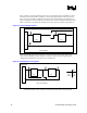
The maximum operating frequency of the scan chain may need to be reduced when a translation
device is placed within the scan chain. Therefore it is recommended to provide a method to bypass
the translated portion of the scan chain to increase the performance of the non-bypassed portion of
the scan chain. When a portion of the scan chain is bypassed, the output enable of the voltage
translator should be held inactive to prohibit bypassed chipset components from acting on debug
port signals intended for the non-translated portion of the scan chain.