
ITP700 Debug Port Design Guide


R
ITP700 Debug Port Design Guide 73
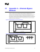
8.3 Intel
®
Itanium
®
2 Processor Routing Guidelines
All of the termination and routing guidelines defined in the multiprocessor chapter of the ITP700
Debug Port Design Guide (found on developer.intel.com) must be adhered to for an ITP700 debug
port implementation with an Itanium 2 processor-based platform with the following clarifications:
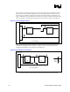
Clarification 1. The BPM[5:0]# and RESET# traces should be terminated to the system bus
termination voltage of 1.2V on both ends of the transmission line. For platforms that make use of
on-die termination of the front side bus on processor and Itanium 2 processor-based chipset
components, please note that the Itanium 2 processors, and Itanium 2 processor-based chipset
components do not provide on-die termination for these signals.
Clarification 2. Itanium 2 processor were designed to support a 1.5 V pull-up voltage for the
JTAG signals. Simulations have shown that these processor inputs will function correctly with a
VTP pull-up of 1.2 V, but the system will have additional noise margin if the VTAP voltage is
1.5 V.
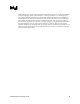
Clarification 3. For Itanium 2 processor-based scan chains, PWR of the ITP debug port must be
pulled up to 1.2 V through a 1.8 kΩ 1% tolerance resistor.