
mPGA604 Socket Design Guide


R
mPGA604 Socket 17
Mechanical Design Guide
4 Electrical Requirements
Socket electrical requirements are measured from the socked-seating plane of the processor test
vehicle (PTV) to the component side of the socket PCB to which it is attached. All specification are
maximum values (unless otherwise stated) for a single socket pin, but includes effects of adjacent
pins where indicated. Pin and socket inductance includes exposed pin from mated contact to bottom
of the processor pin field.
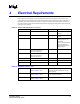
Table 4-1. Electrical Requirements for Sockets
1 Mat lloop inductance, Loop <4.33 nH Refer to Table 4-2, Item 1
2 Mated partial mutual inductance, L NA Refer to Table 4-2,
Item 2a
3 Maximum mutual capacitance, C <1 pF Refer to Table 4-2
Item 3
4 Maximum Ave Contact Resistance ≤ 17 mΩ Refer to Table 4-2, Item 4.
Refer to
Section 4.1 for
more detail.
Refer to mPGA603 Socket
Design Guidelines for
electrical parameters with
INT3 packages.
5 Measurement frequency(s) for
Pin-to-Pin/Connector-to-
Connector capacitance.
400 MHz
6 Measurement frequency(s) for
Pin-to-Pin/Connector-to-
Connector inductance.
1 GHz
7 Dielectric Withstand Voltage 360 Volts RMS
8 Insulation Resistance 800 MΩ
9 Contact Current Rating Read & record
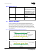
Table 4-2. Definitions (Sheet 1 of 2)
1 Mated loop inductance, Lloop
Refer to
Table 4-1, Item 1
The inductance calculated for two conductors,
considering one forward conductor and one
return conductor.
2a Mated mutual inductance, L
Refer to
Table 4-1, Item 2
The inductance on a conductor due to any
single neighboring conductor.
3 Maximum mutual capacitance, C
Refer to
Table 4-1, Item 3
The capacitance between two pins/connectors.